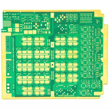
Product name: 20L high-speed PCB
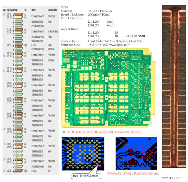
Substrate: TU872LK
Layer: 20L
Finished thickness: 3.2mm
Copper thickness: 1oz (35 μm)
Solder mask: green/white
Minimum line width/line spacing: 4mil/4mil
Surface treatment: electroplated hard gold 3-15u"
Blind hole: L3-L20
Product application: Communication base station backplane
In the field of high-speed PCB, it is widely used in wireless networks, transmission networks, data communications and fixed broadband. Related products include backplanes, high-speed multilayer boards, high-frequency microwave boards, multi-functional metal substrates, etc. The applications of high-speed PCB mainly include wireless networks (communication base stations), transmission networks, data communications and fixed four-part network broadband. Some applications on the market other than wireless networks lack data.
According to calculations, the PCB consumption of a single 5G base station is approximately 3.21 square meters, which is 1.76 times that of a 4G base station (1.825 square meters). At the same time, due to the higher frequency of 5G communication and greater demand for PCB performance, the unit price of 5G base station PCB is higher than that of 4G base station. Generally speaking, the PCB value of a single 5G base station is about three times that of the 4G era.
In addition, due to the higher spectrum of 5G, the coverage area of base stations is smaller. It is expected that domestic 5G base stations will be 1.2-1.5 times that of 4G base stations, and more small base stations will be provided. Therefore, the total number of base stations brought by 5G will far exceed that of 4G. It is expected that the number of new domestic 5G macro base stations during the peak period of 5G construction in 2023 will be 1.5 times that of the peak period of 4G construction in 2015. Based on comprehensive calculations, we believe that the market size of the PCB industry will be approximately 500-260 billion base station communications in the next few years. Compared with the 5-9 billion market in the 4G era, the base station communication PCB industry has undoubtedly experienced explosive growth in recent years.

20-layer high-speed PCB stack-up
When designing high-speed PCB, we often encounter various problems, such as impedance matching, EMI rules, etc. Now I would like to share with you some questions related to high-speed PCB.
1. How to consider impedance matching issues when designing high-speed PCB design schematics?
When designing high-speed PCB circuits, impedance matching is one of the design elements. The impedance value has an absolute relationship with the wiring pipeline, such as whether it is on the surface layer (microstrip) or inner layer (stripline/double stripline), the distance from the reference layer (power layer or ground layer), trace width, PCB material, etc. All will affect the characteristic impedance value of the trace.
That is to say, the impedance value cannot be determined until after wiring. Generally, simulation software cannot take into account some wiring situations with discontinuous impedance due to limitations of the circuit model or the mathematical calculations used. At this time, only some terminators (terminations), such as series resistors, etc., can be reserved on the schematic diagram. To alleviate the effect of trace impedance discontinuity. The real fundamental solution to the problem is to try to avoid impedance discontinuity when wiring.
2. When there are multiple digital/analog function blocks in a PCB board, the common practice is to separate the digital/analog ground. Why?
The reason for separating digital/analog ground is because digital circuits will generate noise in the power supply and ground when switching between high and low potentials. The size of the noise is related to the speed of the signal and the size of the current.
If the ground plane is not divided and the noise generated by the circuits in the digital area is large and the circuits in the analog area are very close, even if the digital-analog signals do not cross, the analog signals will still be interfered by the ground noise. In other words, undivided pipes between digital and analog ground can only be used when the analog circuit area is far away from the digital circuit area that generates large noise.
3. When designing high-speed PCB, from what aspects should designers consider EMC and EMI rules?
Generally, both radiated and conducted aspects need to be considered during EMI/EMC design. The former belongs to the higher frequency part (>30MHz) and the latter belongs to the lower frequency part (<30MHz). So you can’t just pay attention to the high frequencies and ignore the low frequencies.
A good EMI/EMC design must consider the location of the device, the arrangement of the PCB stack, the route of important connections, the selection of the device, etc. at the beginning of the layout. If these are not properly arranged in advance, they will be solved afterwards. It will achieve twice the result with half the effort and increase costs.
For example, the location of the clock generator should not be close to the external connector. High-speed signals should be routed through the inner layer as much as possible. Pay attention to the characteristic impedance matching and the continuity of the reference layer to reduce reflection. The slew rate of the signal pushed by the device should be as small as possible to reduce high voltage. Frequency components, when selecting decoupling/bypass capacitors, pay attention to whether their frequency response meets the requirements to reduce power layer noise.
In addition, pay attention to the return path of the high-frequency signal current to keep the loop area as small as possible (that is, the loop impedance is as small as possible) to reduce radiation. Pipes that separate the formation can also be used to control the range of high-frequency noise. Finally, properly select the chassis ground between the PCB and the housing.
4. When making high-speed PCB board, in order to reduce interference, should the ground wire form a closed sum?
When making high-speed PCB board, it is generally necessary to reduce the loop area to reduce interference. When laying the ground wire, it should not be laid in a closed form. It is better to lay it in a branch shape. In addition, the ground area should be increased as much as possible.
5. How to adjust the wiring topology to improve signal integrity?
The signal direction of this kind of network is more complicated, because the topology affects one-way, two-way signals, and different types of signals with different levels. It is difficult to say which topology is beneficial to the signal quality. Moreover, during pre-simulation, the topology to be adopted is very demanding for engineers, requiring an understanding of circuit principles, signal types, and even wiring difficulty.
6. How to ensure the stability of signals above 100M in high-speed PCB layout and wiring?
The key to high-speed PCB digital signal wiring is to reduce the impact of transmission lines on signal quality. Therefore, when laying out high-speed signals above 100M, signal traces are required to be as short as possible. In digital circuits, high-speed signals are defined by signal rise delay time. Moreover, different types of signals (such as TTL, GTL, LVTTL) have different methods to ensure signal quality.
Product name: 20L high-speed PCB
Substrate: TU872LK
Layer: 20L
Finished thickness: 3.2mm
Copper thickness: 1oz (35 μm)
Solder mask: green/white
Minimum line width/line spacing: 4mil/4mil
Surface treatment: electroplated hard gold 3-15u"
Blind hole: L3-L20
Product application: Communication base station backplane
iPCB Circuit provides support for PCB design, PCB technology, and PCBA assembly. You can request technical consultation or quotation for PCB and PCBA here, please contact email: sales@ipcb.com
We will respond very quickly.