A Trustworthy PCB and Electronic Manufacturing Enterprise! Contact Us


PCB Layout is an important part of PCB design, which mainly involves converting the components and connection relationships in the schematic diagram to the actual PCB board diagram, and carrying out layout and wiring design on the premise of meeting the electrical performance, mechanical performance and manufacturing process requirements.
PCB Layout refers to the process of connecting circuit components and wires between other components into a complete circuit board in circuit board design, that is, circuit board layout. It is usually based on electrical performance, EMC compatible performance, processing feasibility, performance limitation, loss, cost and other factors, and is designed on both sides of the circuit board using the tangent wiring method.
PCB Layout plays a vital role in the electronic manufacturing industry. It is the basis for accurately converting the drawings of electronic components into actual circuit boards. On the one hand, PCB Layout directly affects the connectivity of electronic products. On the other hand, PCB Layout also affects the performance, cost, manufacturing efficiency and other factors of electronic products.

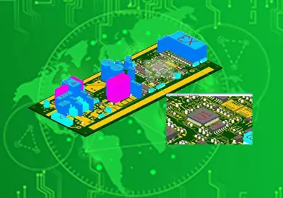
PCB Layout
How to make PCB layout? The basic process of PCB Layout includes the following steps:
1. Understand the basic composition and parameter requirements of the circuit, and determine the basic parameters such as the size and number of layers of the PCB according to the schematic diagram and design specifications.
2. Import the components and connection relationships in the schematic diagram into the PCB design software, which is the basis of layout and wiring.
3. Reasonably place components on PCB according to circuit functions, component attributes, manufacturing process requirements and other factors. The arrangement, direction, spacing and other details of components shall be taken into consideration when layout.
4. Determine the topology, line width, spacing and other principles of cabling according to design specifications and actual requirements.
5. According to the wiring principle, the wiring design shall be carried out for each signal or power supply to be connected, and the principles of minimization, consistency and simplicity shall be followed in this process.
6. Carefully check and correct the design to ensure that all connections are correct and meet the requirements of electrical performance, mechanical performance and manufacturing process.
7. Export design files as manufacturing files, usually including Gerber files, drilling files, etc.

PCB Layout
PCB Layout design service
1. Provide PCB packaging construction for customers for free (customers provide device DataSheet)
2. Provide PCB impedance calculation, stack design, QA inspection, process inspection and EMC inspection for customers free of charge.
3. The design includes high-speed, high-frequency, high-power, analog, digital analog hybrid, HDI, FPC and other design types.
4. Support schematic and PCB software formats: Cadence, Mentor ee, Mentor pads, Altium, AD.
5. IPCB's powerful R&D engineer team provides technical support, assists customers and Layout engineers in schematic analysis and PCB design, eliminates electrical principle design errors, and ensures design quality and reliability.
PCB Layout Design Process
1. The customer provides schematic files and PCB packaging library files, or provides the DataSheet of corresponding devices.
2. The customer provides PCB structure file in DXF format, structure limit description, electrical design description and other precautions.
3. After the start of the project, the engineers of iPCB will check the schematic DRC, check the structure and other electrical design requirements. If there is a problem, they will immediately feed back the EQ to the customer.
4. In the process of project design, iPCB engineers send daily work progress documents to the customer for confirmation. The customer sees the design shape every day, and can timely find problems and deal with them.
5. After PCB layout design is completed, iPCB engineers conduct mutual inspection, including DFM inspection, QA inspection, EMC inspection. After the customer confirms that it is OK, Gerber and other production documents are issued.
6. After the customer confirms that it is OK, iPCB engineers output ASM assembly documents, SMT placement documents, PCB design original documents, Gerber documents, EQ engineering communication records, etc.
Professional PCB layout software, such as Altium Designer, Cadence, Mentor Graphics, is required for PCB layout. These powerful software can complete complex layout and routing design tasks.
If multi-layer board design or high-speed, RF, antenna and other high-frequency PCB design is carried out, EMI, FCC, CE and NCC specifications need to be followed. It is recommended to find a PCB Layout company with relevant design expertise.