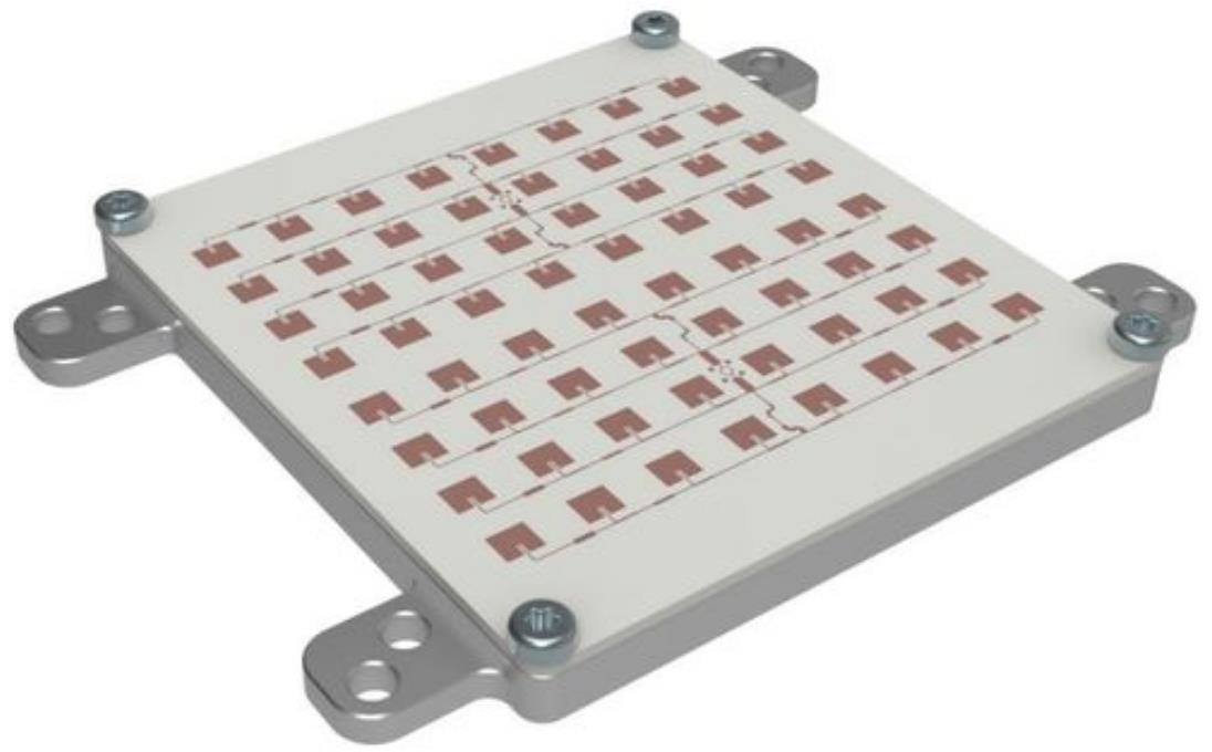
In the frequency band greater than 10GHz, PCB microstrip antennas have obvious advantages over other antennas such as waveguide slit antennas, lens antennas, reflective surface antennas, and so on. Mature PCB processing technology can effectively control the production cost of microstrip antennas. The multi-layer hybrid technology of microstrip antenna circuit boards, microwave RF boards and low-frequency digital-module circuit boards also makes the whole RF system highly integrated.
ROGERS microwave RF board RO4350B has superior high frequency performance and low production cost, and has been widely used and proven in commercial RF systems. The author used Rogers circuit board Rogers RO4350B successfully designed a series of 24GHz microstrip array antenna, have been applied to the company's listed products, so the application of some of its design skills summary.
High Frequency PCB Material Thickness Selection
Thickness is mainly based on the microstrip antenna operating bandwidth, feed network design and antenna efficiency of three factors to choose.
1.PCB thickness affects the impedance bandwidth of the microstrip antenna.The smaller the PCB thickness, the larger the array size, the smaller the operating bandwidth of the microstrip antenna.
2.The thickness of the dielectric affects the conductor loss of the microstrip line, which in turn affects the efficiency of the microwave RF antenna.Based on the above factors, the author's design experience is to choose 10mil or 20mil thickness for small arrays, 20mil thickness for large arrays, and 10mil thickness for microwave RF boards.
3.The thickness of the PCB determines the width of the microstrip line in the impedance change section of the feed network.For RO4350B PCB, the thickness of 20 mils, 50Ω and 100. Ω microstrip line line width of 1.13mm and 0.27mm, respectively, the corresponding microstrip antenna resonance length at 24GHz is about 3mm. If the impedance of the microstrip conversion section of the feed network is too small or too large, it will cause the microstrip antenna line is too wide or too narrow, the microstrip antenna line is too broad, which is prone to cause structural interference. If the microstrip antenna line is too wide, it will easily cause structural interference. If the microstrip antenna line is too narrow, it will cause processing difficulties.

Antenna Board
Antenna Types
Microstrip array antennas are classified into parallel feed arrays and series feed arrays based on the feed path. Parallel-fed arrays have longer feed lines, resulting in higher losses in the feed network. For large-scale arrays, antenna efficiency is often limited, so the simpler series-fed array is generally preferred. Series-fed arrays are resonant antennas that operate over a smaller bandwidth than parallel-fed arrays, but the series-fed structure makes it easier to achieve weighted excitation. The authors have designed series-fed microstrip array antennas of different scales. They all use 20 mil thick RO4350B. The impedance bandwidth decreases as the array size gets larger. The bandwidth is 1.2 GHz for 16 arrays and only 0.75 GHz for 324 arrays. The impedance bandwidth of this tandem-fed array meets most of the system design requirements for a 24 GHz radar frequency modulation bandwidth of less than 250 MHz, which is typically used in continuous wave systems.
Interconnection between antenna and RF chip
Currently,24GHz RF chips have been mass-produced in the market by domestic and foreign chip manufacturers. In the Zero IF radar architecture, the pins of the RF chip are directly connected to the microstrip transceiver antenna port. In the case of an antenna board (HF board) + multilayer FR4 + microwave RF board (HF board), the antenna and the RF chip are interconnected through metallised vias. In the 24GHz band, the discontinuity introduced by the metallised vias with a length greater than 1mm is very obvious.The solution is to add several symmetrical metallised ground vias around the metallised vias to form a coaxial-like transmission structure. When the antenna and RF chip are located on the same side of the PCB, the RF chip and the transceiver antenna are directly connected via a microstrip line or coplanar waveguide.This design minimises the insertion loss of the transmission line.
Low Subflap Design
The sub-flap level of the directional map is an important part of the design of an array antenna.The low flap design reduces the environmental interference outside the main beam of the radar. Its function is equivalent to a spatial filter, which is very effective in improving the radar signal-to-noise ratio. Uniformly distributed array antennas have a flap level greater than -13dB. In order to obtain a low flap, the power fed into each array element is distributed through a feed network to form a certain low flap weighted distribution. Commonly used methods for equal-phase unequal-amplitude low-paraflap weighted distribution include the Chebyshev and Taylor distributions. According to the paraflap level and the number of array elements, it is easy to synthesise the ideal weighted distribution. The rest of the work is to optimise the feed network iteratively so that the power fed into each array element is close to the ideal distribution.