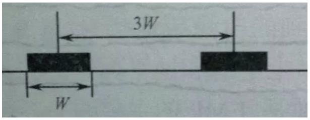
Crosstalk refers to the mutual interference between different networks on the PCB caused by longer parallel lines, mainly due to the distribution of capacitance and inductance between parallel lines.
The main measures to overcome crosstalk are:
1.New parallel line spacing, follow the 3W principle.
2.Insert a grounding isolator between parallel wires.
3.Reduce the distance between the wiring layer and the ground plane.

3 W Rule
In order to minimize crosstalk between wires.the spacing between wires should be large enough.When the distance between wire centers is not less than 3 times the wire width.70% of the electric field can be maintained without interference.which is called the 3W rule.To achieve 98% non-interference of electric fields.10W spacing can be used.
In actual PCB design.the 3W principle does not fully satisfy the requirement of avoiding crosstalk.
According to practical experience.if there is no mask ground.the distance between the signal lines printed above to be greater than the LCM to prevent crosstalk.so in the PCB circuit wiring.the need for noise signals (such as clock lines) and noise signals.and EFTlB.“dirty” “clean “ and other ESD interference need on-line protection.not only to mandatory use of the 3W principle.but also to the ground packet masking process to prevent crosstalk.
In addition.in order to avoid crosstalk in the PCB.PCB design and layout.should be considered for example:
1.According to the function of the logic device series.strict control of the bus structure.
2.Minimize the physical distance between components.
3.High-speed signal lines and components (e.g..crystals) should be located far away from areas susceptible to data interference and coupling.such as I/() interconnect interfaces.
4.Provide correct wiring terminals for high-speed circuits.
5.Avoid parallel wiring over long distances and provide sufficient spacing between wires to minimize inductive coupling.
6.Neighboring layers (microstrip or strip) on the wiring should be perpendicular to each other to prevent interlayer capacitive coupling.
7.Reduce the distance between the signal and the ground plane.
8.Separate and isolate high noise emitters (clocks.I/O.high-speed interconnections).and distribute different signals on different layers.
9.As much as possible to increase the distance between the signal lines.can effectively reduce the capacitive crosstalk.
10.Reduce the lead inductance.avoid using high impedance loads and low impedance loads in the circuit.and try to stabilize the load impedance of the analog circuit between loQ~lokQ.Because high impedance loads will add capacitive crosstalk.when using very high impedance loads.due to high operating voltage.capacitive crosstalk will be added.and when using very low impedance loads.due to high operating current.inductive crosstalk will be added.
11.High-speed cycle signals are laid on the inner layer of PCB board.
12.The use of impedance matching technology to ensure the integrity of the BT signal to prevent overshooting.
13.Pay attention to the fast rising edge (tr ≤ 3ns) of the signal.grounding anti-crosstalk processing.PCB edge layout of some of the EFTlB or ESD interference and has not been filtered signal line.
14.Use ground plane as much as possible.Signal lines using the ground plane will be attenuated 15~20dB than those not using the ground plane.
15.Signal high frequency signals and sensitive signals are included in the ground processing.dual-panel use of ground cover technology.attenuation 10 ~ 15dB.
16.Use balanced line.mask line or coaxial line.
17.Filter the disturbing signal lines and sensitive lines.
18.Reasonable setup of layers and wiring.reasonable setup of layers and spacing of wiring.reduce the length of parallel signals.Reduce the spacing between signal layers and planar layers.increase the spacing of signal lines.reduce the length of parallel signal lines (within the range of key lengths) can effectively reduce crosstalk.
The 3W principle is a way to prevent crosstalk.and the method is only used as a reference and an inspiration to understand how to prevent crosstalk.In actual PCB design.the 3W principle does not fully satisfy the requirement of avoiding crosstalk.According to practical experience.if there is no mask ground.the distance between the PCB signal lines is more than lcm to prevent crosstalk.so when laying out the PCB circuit.it is necessary to lay out the signal lines between the noise source signals (such as the clock alignment) and the non-noise source signals.as well as the “dirty” lines that are subjected to the interference of the EFT.ESD.and so on.and the “clean” lines that need to be protected.Between the “dirty” lines and the “clean” lines that need to be protected.not only should the 3W principle be mandatory.but also the mask ground wrap treatment should be carried out to prevent crosstalk from occurring.In addition.not all PCB alignments must follow the 3W principle.Using this design guideline.it is important to decide which alignments must use the 3W principle before PCB routing.