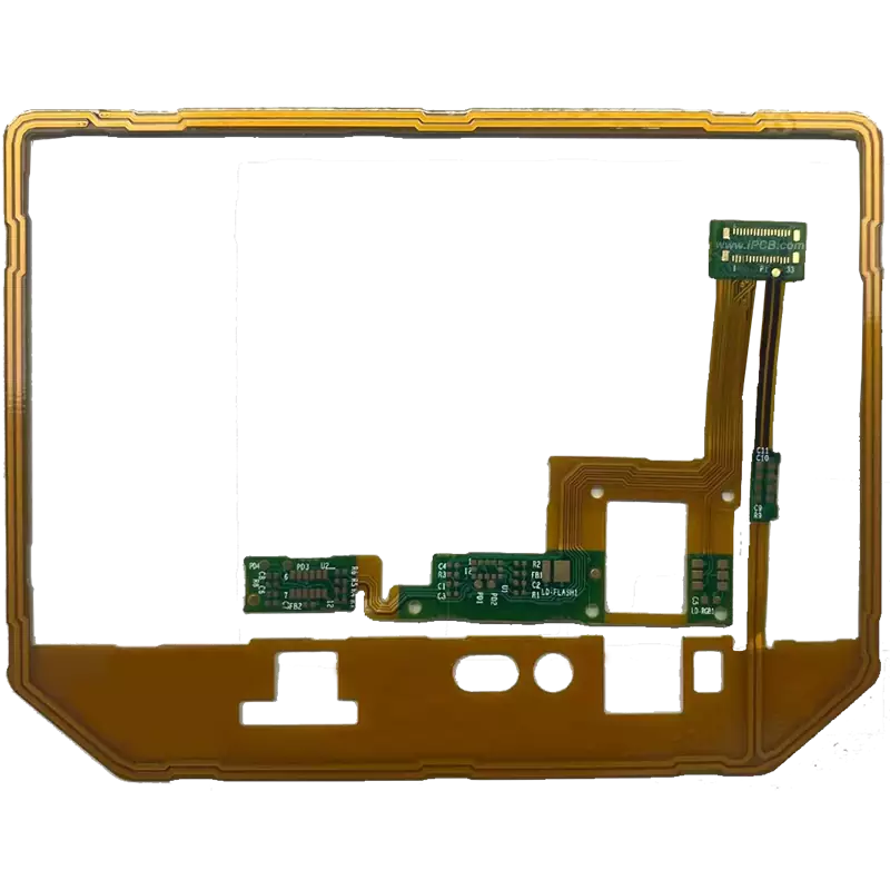
Product Name: 4-layer Rigid-Flex PCB
Substrate: FR4+PI
Layer: Rigid 2L+Flex 2L
Copper thickness: 1oz (35 μ m)
Finished thickness: 0.6mm
Surface treatment: Immersion Gold
Thickness gold: 2μ"
Minimum line width/spacing: 4/4 mil
Minimum aperture: 0.2mm
Product application: Display screen, Touch screen
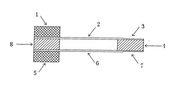
The 4-layer Rigid-Flex PCB stacking design includes a double-layer flexible PCB, a gold finger located on one end of the flexible PCB, two layers of rigid PCBs respectively located on the outer side of the other end of the flexible PCB, FR4 between the double-sided gold fingers on the end side of the double-layer flexible PCB, and FR4 between the two layers of flexible PCBs at the rigid PCB. The area between the double-layer flexible PCBs in the middle of the two FR4 is hollow, which is a layered structure of FPC. This structure gives the gold fingers of the flexible PCB a certain thickness and maintains strong rigidity, while the middle part of the FPC connecting the hard board has good flexibility. This entire structure can ensure multiple insertions and removals of the gold fingers of the flexible PCB, as well as ensure that the middle part of the FPC connecting the hard board has good flexibility. The electrical connection of the entire product, while maintaining the flexural performance of the middle part of the FPC.
There are many flexible PCB connections with gold fingers in the current Rigid-Flex PCB structure. In this structure, some FPCs have good flexibility, but the gold fingers of FPCs are too soft, which is not conducive to multiple insertions and removals Some FPC base end gold fingers have rigidity and are easy to plug and unplug, but the connected FPC is not flexible enough, which makes it difficult for the gold fingers of flexible PCB to be plugged and unplugged multiple times, thereby affecting the plugging and unplugging effect.
Specifically, the structural design of the 4-layer Rigid-Flex PCB includes:
1. Double layer flexible PCB: This is the basic part of Rigid-Flex PCB, which is equipped with gold fingers and two layers of rigid PCB
2. Golden finger: located on one end of the flexible PCB, used for electrical connection with other electronic components
3. Two layers of rigid PCBs: located on the outer side of the other end of the flexible PCB, serving as input and output interfaces for the circuit board
4. FR4: FR4 between the double-sided gold fingers on the end side of the double-layer flexible PCB and FR4 between the two layers of flexible PCB at the rigid PCB
5. FPC layered structure: The area between the double-layer flexible PCB in the middle of two FR4 blocks is hollow, forming an flexible PCB layered structure. This structural design gives the flexible PCB's gold fingers a certain thickness, maintaining strong rigidity, while the middle part of the FPC connecting the hard board has good flexibility.

4-layer Rigid-Flex PCB stack-up
This structural design can meet the following requirements:
1. Ensure multiple insertions and removals of flexible PCB gold fingers
2. Ensure the electrical connection of the entire product
3. Maintain the flexural performance of the middle part of the FPC.
This 4-layer Rigid-Flex PCB stacking design not only achieves high performance, high reliability, and high integration of the circuit board, but also considers the manufacturability and maintainability of the product.
Product Name: 4-layer Rigid-Flex PCB
Substrate: FR4+PI
Layer: Rigid 2L+Flex 2L
Copper thickness: 1oz (35 μ m)
Finished thickness: 0.6mm
Surface treatment: Immersion Gold
Thickness gold: 2μ"
Minimum line width/spacing: 4/4 mil
Minimum aperture: 0.2mm
Product application: Display screen, Touch screen
iPCB Circuit provides support for PCB design, PCB technology, and PCBA assembly. You can request technical consultation or quotation for PCB and PCBA here, please contact email: sales@ipcb.com
We will respond very quickly.