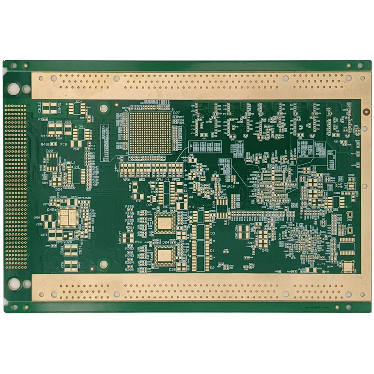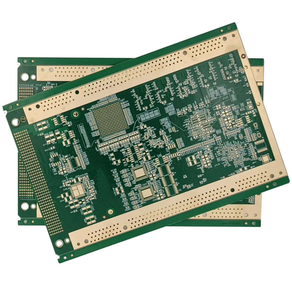

Product: 6 Layers PCB
Material: SY S1000-2
Layer: 6
Color: Green/White
Finished thickness: 1.6mm
Copper thickness: 1/H/H/H/H/1oz
Surface treatment: immersion gold
Minimum line width: 4mil
Minimum spacing: 4mil
Impedance requirement: Yes
Application: Control Circuit
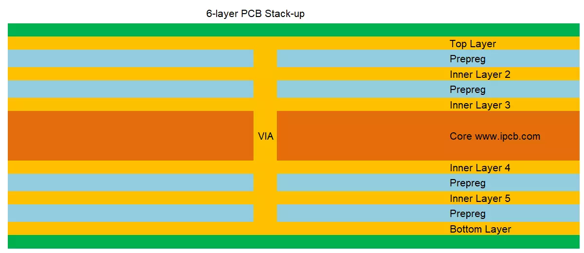
6 layer PCB is a very common circuit board design, which is based on the principle of arranging electronic components and wires on six circuit layers to achieve circuit connections and functions.
The layering of a 6layer PCB is achieved by inserting laminates into the board, dividing the entire circuit board into multiple different layers. These layers include: Top Layer, Inner Layer 2, Inner Layer 3, Inner Layer 4, Inner Layer 5, Inner Layer 5, and Bottom Layer. The top and bottom layers are the outermost layers used for arranging electronic components and connecting circuits, while the remaining four layers are used for detailed circuit layout and power distribution.
Why do we need a 6 layer PCB design?
This is because PCB layered design can bring many benefits. Firstly, layering can increase the degree of freedom in wiring, making the routing of lines on the circuit board more flexible. Secondly, layering can effectively reduce signal interference. By arranging power and ground planes in the inner layer, a composite layer structure of "power ground power ground" can be formed, providing good power and ground guidance and reducing mutual interference in signal transmission. In addition, through reasonable layered design, the signal transmission path can be shortened, and the response speed and reliability of PCB circuit boards can be improved.

The layered design of a 6 layer PCB plays an important role in the performance and reliability of the circuit board. Through the layered design of circuits, flexibility in circuit wiring can be achieved, signal interference can be reduced, and signal transmission speed and reliability can be improved.
Product: 6 Layers PCB
Material: SY S1000-2
Layer: 6
Color: Green/White
Finished thickness: 1.6mm
Copper thickness: 1/H/H/H/H/1oz
Surface treatment: immersion gold
Minimum line width: 4mil
Minimum spacing: 4mil
Impedance requirement: Yes
Application: Control Circuit
iPCB Circuit provides support for PCB design, PCB technology, and PCBA assembly. You can request technical consultation or quotation for PCB and PCBA here, please contact email: sales@ipcb.com
We will respond very quickly.