EMC stands for Electromagnetic Compatibility. EMC in PCB refers to the ability of a circuit board to operate in its electromagnetic environment without causing unbearable electromagnetic interference to other surrounding devices. It includes two aspects, one is interference with other electrical products, abbreviated as EMI (electromagnetic interference), that is, electromagnetic interference; Another type is interference from other electrical products, called anti-interference, which we use EMS (electromagnetic compatibility) to refer to explain.
Generally seaking, to achieve EMC compliant design, engineers need to consider three basic aspects:
Generating unwanted electromagnetic radiation and its propagation.
The vulnerability of each design or component to electromagnetic interference.
PCB design should not cause intolerable electromagnetic interference to itself.
The Three Elements and Countermeasures of Electromagnetic Compatibility
To address electromagnetic compatibility issues, we need to start with three key elements: interference sources, coupling pathways, and sensitive devices.
Interference sources are the sources of electromagnetic interference, commonly found in clock circuits, switching power supplies, high-speed buses, and inductive devices. For example,the crystal oscillator in the clock circuit generates high-frequency signals, which, if not controlled, may interfere with other circuits.
The coupling pathway is the channel through which electromagnetic interference propagates, including conducted interference and radiated interference. Conducted interference is noisethat propagates through power or signal lines, while radiated interference is directly emitted in the form of electromagnetic waves. For example, power lines may transmit interference signals
to other devices, while high-speed signal lines may emit electromagnetic waves like antennas.
Sensitive devices are circuits or components that are susceptible to electromagnetic interference. For example, crystal oscillators, reset signals, and weak signals are all sensitive parts
Measures to address these three elements:
Reducing interference sources: By optimizing circuit design, such as using clock spread spectrum technology or slowing down the rising edge of signals, interference strength can be effectively
reduced. At the same time, selecting components reasonably and reducing antenna effects can also control the generation of EMI.
Cut off or weaken the transmission pathway: For conductive coupling, filtering capacitors, filters, or isolation transformers can be added; For radiation coupling, interference can be reduced through
reasonable layout, wiring, and shielding measures.
Improving the anti-interference ability of equipment: By necessary layout, wiring, and grounding measures, the equipment's resistance to electromagnetic interference can be enhanced.
Electromagnetic Compatibility Strategy in PCB Design
Electromagnetic compatibility is an important consideration throughout PCB design. Reasonable PCB design can not only effectively solve electromagnetic interference problems, but also improveequipment performance and reliability.
Layer design: Building a stable electromagnetic environment
The layer design of PCB is the foundation of electromagnetic compatibility. Reasonably determine the number of wiring layers and the number of power and ground layers based on the density
of single board wiring and signal requirements. Generally speaking, the layer adjacent to the component surface should be the ground plane, which can provide a reflow plane for top-level wiring
and also serve as shielding. All signal layers should be adjacent to the ground plane as much as possible, ensuring that critical signal layers are adjacent to the ground plane to reduce electromagnetic
interference. The main power layer should be adjacent to its corresponding layer to avoid direct adjacency between the two signal layers and reduce crosstalk. In addition, the laminated structure
should be as symmetrical as possible to ensure the stability of the PCB.
Avoid crosstalk
Crosstalk is used to identify interference caused by electromagnetic noise from one track on a PCB to another nearby track. Crosstalk in PCBs usually occurs on adjacent tracks in the same layer
or on one track in adjacent layers. This situation manifests as noise, and if the amplitude is too large, it may cause malfunctions.

Avoid crosstalk
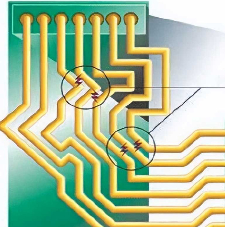
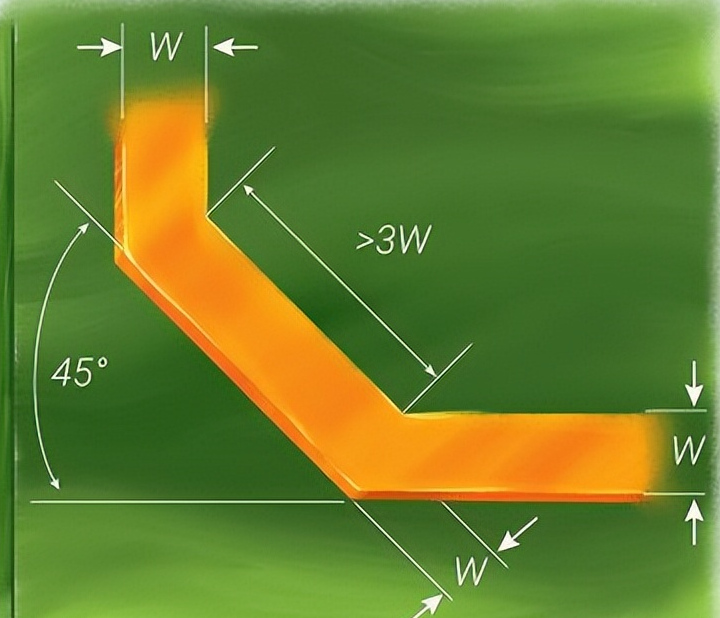
Do not run the wire at a 90 degree angle
Similar to through holes, 90 ° right angle track turns should not be implemented as it increases parasitic capacitance, causing changes in characteristic impedance and resulting in reflections.
As shown in the figure, all orthogonal traces should be bent at a 45 ° angle to limit the noise coupled to nearby traces.

Not run the wire at a 90 degree angle
Layout: Reasonable partitioning to reduce interference
When laying out PCBs, it is necessary to partition them according to functional modules, and separate the layout of digital circuits from analog circuits, high-speed circuits from low-speed circuits.
For example, placing strong radiation devices or sensitive devices such as crystals, crystal oscillators, relays, etc. away from external interface connectors is recommended at a distance of ≥ 1000mil.
The layout of the interface circuit is also very important, and filtering, protection, and isolation devices should be placed near the interface connector, following the principle of protection first and filtering
later. The layout of the clock circuit also needs special attention. The clock driver should be placed close to the crystal oscillator, and the matching resistor of the clock output should be close to the output
pin of the crystal oscillator or clock driver circuit. The recommended distance is ≤ 1000mil.
Wiring: Optimize paths to reduce interference propagation
Wiring is a crucial step inPCB design, and proper routing can effectively reduce the propagation of electromagnetic interference. Prioritize the use of inner layer wiring to avoid signal lines crossing
over segmented areas. The wiring of interface circuits should follow the principle of protection before filtering, and differential signal lines should strictly follow the rules of differential distribution lines
to ensure parallelism, same layer, and equal length. The wiring requirements for clock signals are more stringent, and the surface wiring length should be as short as possible. The recommended length
for critical clock surface wiring is ≤ 200mil, and there should be a complete ground plane for reflow. Other signal lines should be avoided around the clock signal line, and it is recommended to follow the
3W principle.
Grounding and Shielding: Building Electromagnetic Protection Walls
Grounding and shielding are important means in electromagnetic compatibility design. Good grounding can provide a low impedance path for electromagnetic interference and reduce the propagation
of interference signals. For example, by setting a large area of ground plane on the PCB, electromagnetic interference can be effectively reduced. Shielding can be achieved through a metal shielding
layer or shielding cover to isolate the interference source from the sensitive circuit. For example, setting up shielding covers around high-speed signal areas or strong radiation devices can effectively reduce
the propagation of electromagnetic interference.