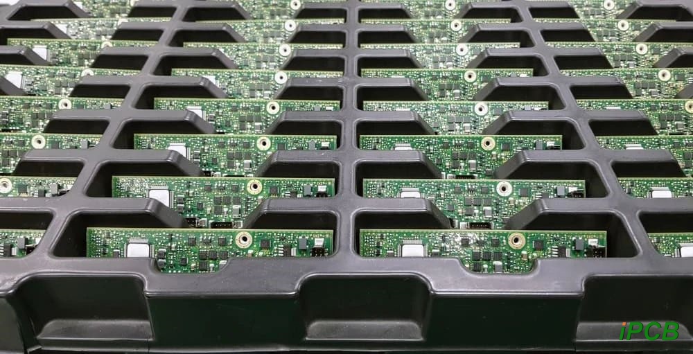
The electrical parts assembly and soldering process turns a circuit board into a functional prototype. The PCB assembly (PCB assembly, or PCBA) phase includes device placement, soldering, inspection, and finally testing. The PCBA process can be a manual or automated process, which is determined by the manufacturer at each stage.
There are three technologies used in the PCBA process, which are discussed below.
Electrical parts assembly technologies In the PCBA process, there are three key technologies:
Through hole technology (THT) PCBA process
In through hole technology, pinned or plug-in electronic devices are soldered to the circuit board to form a circuit. The leads or terminals of the device are inserted through holes or pads on the PCB and soldered on the other side.
Surface mount technology (SMT) PCBA process
There are two types of pads: through-hole and surface mount. In a PCB using surface mount pads, surface mount devices (SMDs) are soldered to form a circuit. The soldering surface is also the surface on which the device is placed with the help of solder paste.
Mixed Technology PCBA Process
As circuit designs become more complex, it is impossible to stick to only one type of device in the circuit. In PCBs that implement complex circuits, there are both plug-in and surface mount devices. This PCB that uses mixed devices is called a mixed technology circuit board, and its assembly process uses the mixed technology PCBA process.

Steps of Through-Hole Technology PCBA
The order of the PCBA process varies depending on the mounting technology used. Now let's discuss the steps of through-hole technology PCB assembly.
01 Component placement: In through-hole technology PCBA, engineers first place the components in the corresponding positions given in the PCB design file.
02 Inspection and correction: After all components are placed, the circuit board should be inspected. During the inspection, check whether the components are placed accurately. If the components are found to be placed inaccurately, such problems should be corrected immediately through the correction steps. Inspection and correction must be completed before the welding process.
03 Soldering: The next step of the process is welding, which fixes the placed components on the corresponding pads.
04Testing: After the PCB assembly and soldering process is complete, the board can be tested. Every PCB board used in electronic equipment goes through this process and passes the test.
Best Practices for Improving the Electrical Parts Assembly Process
1 Optimize the Device Selection Process
Avoid using exotic devices, which are hard to find and may slow down the board building process. In addition, unless both are necessary, choose one of the THT or SMT devices.
2Don't Overload the Net
Overloaded nets mean heavy copper weight on the board, which may require wider traces and may cause clearance challenges.
3Follow device, trace, and edge clearance rules
Clearance is used to ensure that soldering and panelization can be done easily. In addition, insufficient clearance can also cause electromagnetic interference problems, affecting operation and performance.
4Use the minimum number of layers in the stackup when sufficient is guaranteed
Extra layers increase the height of the board, which not only affects the housing design, but also increases the material cost of large-volume production orders.
5Perform DFA and DFM checks frequently
All DFM and DFA violations should be avoided as much as possible, so checks need to be performed frequently during design. Additionally, DRC checks are often prioritized, meaning that lower priority issues may be difficult to clear if they are postponed to the end of the design.
6 Consider heat dissipation and distribution
The soldering process depends on adequate distribution and dissipation of heat. Therefore, it is best to perform thermal simulations, including power distribution analysis, to ensure that there are no hot spots on the board.
7 Ensure the design package is accurate and complete
Whether using traditional Gerber files or ECAD models, board manufacturing (including the PCB assembly process) relies on the accuracy and completeness of the design package, and any special instructions that need to be incorporated should be provided.
8 Ensure the bill of materials matches the board footprint
Similar to the design package, the bill of materials component information must match the layout parameters; for example, MPN, correct device footprint, and pads.
9 Work with the contract manufacturer to ensure that the design intent is fully communicated
Engaging with the contract manufacturer early and establishing transparent communication is the best way to ensure that the design intent is incorporated into the entire board build.
10 Understand the importance of design decisions to thePCB assembly process
In addition to the contract manufacturer understanding the design intent, designers should also understand how their choices affect the PCB assembly process.
Electronic parts assembly is a meticulous art that brings electronic systems to life. Every connection,every component placement requires precision and expertise to ensure functionality and reliability. As technology continues to evolve, mastering this craft becomes increasingly important.