HDI PCB, or High-Density Interconnect Printed Circuit Boards, are circuit boards manufactured using advanced technology characterized by a higher wiring density per unit area than conventional printed circuit boards HDI PCBs typically employ micro-blind and buried hole technology, which results in a significantly higher density of line distribution. Due to this layout, HDI PCBs can effectively reduce size and weight to meet the demand for compact designs in modern electronics.
As defined by IPC-2226, these boards use thinner wires and smaller gaps (≤ 100 µm/0.10 mm) to achieve higher electrical connectivity, increased board space utilization, and improved signal transmission speed and quality.
HDI PCBs' requirements for production stackup
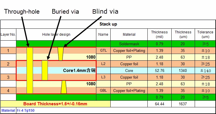
HDI PCBs are typically constructed with 4 or more layers. Stacked layer design requires optimized interlayer connections, i.e., the use of blind and buried vias to improve electrical performance and reduce board thickness, as well as consideration of routing widths, via sizes, and interlayer space to ensure signal integrity and minimize electromagnetic interference. Regarding board selection, FR-4 materials are typically used, which have low dielectric constants and small coefficients of thermal expansion (CTE) to effectively reduce signal transmission losses in high-density layouts. For specialized applications, such as aerospace or military use, higher-performance materials may be used to ensure reliability under extreme conditions. So, the HDI PCBs' production stackup should be combined the actual manufacturing technology.

HDI PCBs' production stackup
Limitations of laser drilling for HDI PCB production
There are several technical limitations to the laser drilling of HDI PCBs. These limitations are primarily related to the thickness of the board, the aperture, and the manufacturing process. Laser drilling technology has definite limitations on the thickness of the board. Specifically, the dielectric thickness of the board is usually limited to 0.13 mm, beyond which the drillingoperation cannot be performed effectively. Laser drilling generally requires a hole diameter of 3-5 mil (about 0.076-0.127 mm) between, for through-blind holes, especially high-end HDI boards, the hole diameter is often less than 0.1 mm. Otherwise, not only affects the speed of production but alsogreatly affects the production yield.
In addition, before laser drilling, the copper layer on the board needs to be etched with a Cu Clearance that matches the finished aperture diameter. This is because it is extremely difficult for the laser to penetrate the copper material, which, if not handled properly, can lead to a reduction in the quality of the drilled holes.
HDI PCBs are widely used in modern electronics, including smartphones, tablets, high-speed networking devices, and other devices with stringent performance and space requirements. The production process for HDI PCBs is more complex than that for PCB Board and involves multiple steps, requiring strict control at every step to ensure the quality of the final product.