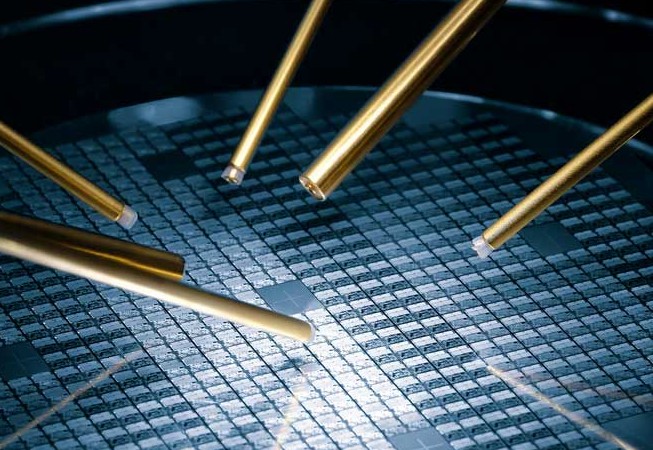
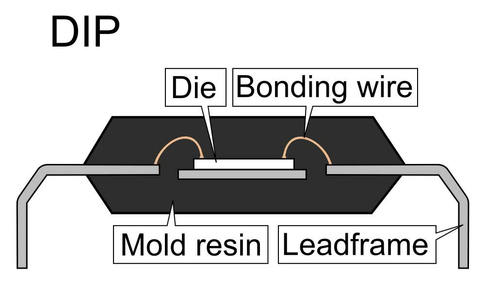
IC substrate is used to encapsulate the bare wafers of integrated circuits (ICs), featuring high density, high precision, high performance, miniaturization and thinness, etc. It is used to forma chip together with die and lead wires after encapsulation and testing. The main role includes carrying the wafers, providing heat dissipation, protection, and fixation of the chip, and at thesame time between the chip and the PCB to provide electronic connectivity. In general, the IC substrate plays a role in supporting the chip, but also plays a role in the electrical connection.
The technical characteristics of IC substrates include miniaturization, high density, multifunctionality, low power consumption, and high reliability. The current microvia aperture requirement reaches 50 to 100 microns with a line width pitch of 20 to 50 microns.

IC substrates can often be categorized based on material, structure, and function. Its main types include:- Rigid package substrate: mainly made of epoxy resin, BT resin, or ABF resin, which is the most widely used- Flexible package substrates: usually made with polyimide (PI) or polyester (PE) resins, suitable for application scenarios that require flexibility and thinness-Ceramic Package Substrates: Composed of ceramic materials such as alumina, aluminum nitride, or silicon carbide, they provide better thermal stability and lower coefficient of thermal expansion.
IC substrates are widely used in mobile communications, automotive electronics, and consumer electronics. For example, in 5G communication devices, IC substrates not only need to support high-frequency signal transmission but also need to have good heat dissipation performance to meet the demand for high performance in smart devices. With the rapid developmentof the IoT and smart device markets, the market demand for IC substrates continues to grow.
The production of IC substrates faces multiple constraints, including technical barriers, material selection, complexity of the manufacturing process, and rapid changes in market demand. The production of IC substrates is technically very demanding, involving complex manufacturing processes and sophisticated production equipment. The existence of technical barriers makes it difficult for some small enterprises to enter the market, further exacerbating the competitive imbalance in the industry. The manufacturing process of IC substrates is very complex and requires a high level of technical support. Each step in the production process must ensure high precision, high density, and stability. These factors affect the manufacturing yieldand cost of IC substrates.
In addition to the production of IC substrates, it also involves a very important production technology - IC and wafer bonding technology, based on which IC substrates and wafers can be combined and the electrical performance of the product can be realized.

IC bonding technology mainly refers to the process of electrically connecting the IC chip to the carrier board during the semiconductor packaging process. Binding technologies include COB (Chip-on-Board) and Flip Chip, which provide efficient electrical connections between the connected chips and the substrate.
- CHIP ON BOARD (COB): IC soft packaging technology, bare chip packaging or bonding (Bonding), that is, the chip is pasted directly to the circuit board, to achieve the indirect connectionline reduced to a minimum. This technology can significantly reduce the size of the package, and improve the overall integration and performance.
- Flip Chip: The chip is flipped on its front side, and the bumps are directly connected to the carrier board in the package form. In this technology, the contact point of the chip is located at its bottom and is connected to the carrier board through small solder bumps.