A Trustworthy PCB and Electronic Manufacturing Enterprise! Contact Us


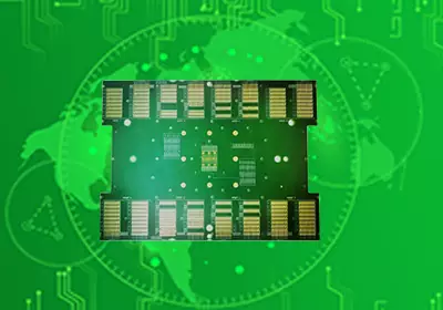
IC and PCB are two halves of every electronic product: the integrated circuit does the thinking, and the printed circuit board gives it power, signals and a place to live. Most design trouble shows up where the two meet, in a footprint that is slightly off, a package that overheats, or a board that cannot route the chip’s pins. This article looks at that meeting point, with a focus on the choices that affect cost, yield and lead time when you order boards for IC board components.
It helps to start with what each side is. An integrated circuit is a tiny slice of silicon holding thousands to billions of transistors, sealed in a package so it can be handled and soldered. A PCB is a laminate of copper and glass-epoxy that wires those packages together. The chip does not care what board it sits on, but the board very much cares what chip you pick. A 0.4 mm pitch BGA needs fine lines, small vias and tight registration. A simple 8-pin op-amp needs almost nothing. Knowing the difference is the first step in choosing IC board components that your fabricator can build reliably.
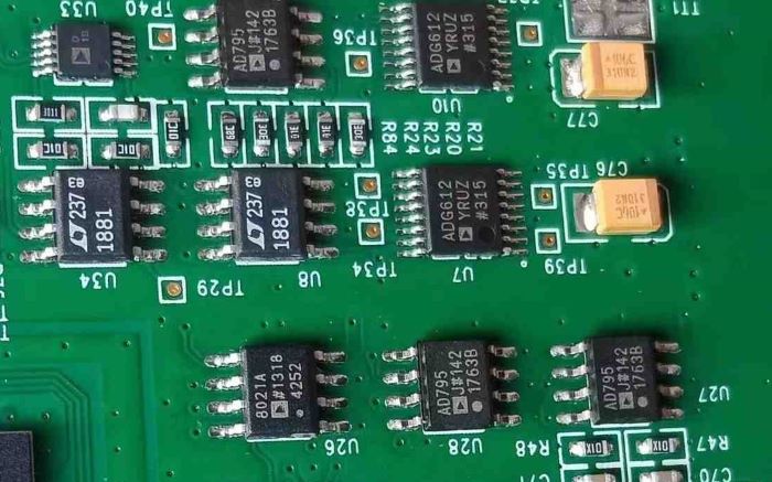
Package type decides most of what the board must do. Through-hole packages such as DIP are easy to solder by hand but take space. Leaded surface-mount parts like SOIC and QFP bring pins around the edge, so the board needs pads along each side and enough room between them for solder mask. QFN packages have pads underneath, which saves area but hides the joints. BGA parts hide the entire array of balls below the body, so routing has to escape from the center and the board often needs more layers. When people ask why a design needs a multilayer PCB, the answer is often one BGA with too many pins and not enough room.
Pitch and routing
Pitch, the distance between pin centers, is the number that links chip and board. At 1.27 mm you can run a trace between pads without much thought. At 0.8 mm you can still do it with thin lines. At 0.5 mm and below, you are into fine-line work, microvias and often via-in-pad, and the cost of the board rises with each step. Ask your supplier what they hold in volume, not only what they can do on a good day. A capability listed as 3 mil trace and space may drop in yield on large panels.
Escape routing is the practical side of this. With a dense BGA, the outer rows come out on the top layer, and the inner rows need to dive through vias to deeper layers. Dog-bone vias work down to roughly 0.8 mm pitch. Finer than that, designers move to via-in-pad, where the via sits inside the pad and is filled and plated over, so solder does not wick down into the hole. This adds a process step, and it is worth confirming early that your board shop does it routinely, not as a special.
Power, heat and the board stack-up
A chip draws current in sharp bursts, and the board has to deliver it without voltage dips. That is the job of decoupling capacitors, which should sit as close to the power pins as possible, with short, wide connections to the planes. A thin dielectric between power and ground planes adds a little distributed capacitance that helps at high frequency. In practice, many fast designs use a stack-up with solid ground planes next to every signal layer and a closely coupled power pair.
Heat is the other half. A processor or power IC can dissipate several watts, and the board is usually the main path out. Exposed thermal pads on QFN and some BGA packages should connect to a copper area through an array of thermal vias. Too few vias and the chip runs hot. Too many open vias under the pad can wick solder away during reflow and leave voids. Plugged or capped vias help, and so does a sensible paste stencil design that breaks the thermal pad into small windows.
Surface finish and assembly
The finish on the pads matters more for fine-pitch IC work than for ordinary boards. Lead-free HASL leaves a slightly uneven surface, which is fine for coarse parts and unreliable for 0.5 mm pitch. ENIG gives a flat, solderable pad that suits QFN, BGA and fine-pitch QFP, and its shelf life is good. Immersion silver and tin work too but need tighter control of storage and handling. Match the finish to the finest part on the board.
Solder mask is the quiet detail that causes trouble. Between two pads at 0.4 mm pitch, there may be only 0.1 mm of space for a mask dam. If the mask openings are too generous, there is no dam and solder bridges between pins. If they are too tight, registration errors cover part of the pad. Tell your fabricator the finest pitch on the board, and ask what mask dam width they can hold.
On the assembly side, the stencil, the paste and the reflow profile have to match the packages. Thin stencils, around 0.1 mm, suit fine-pitch parts. BGA balls need enough paste for a good joint and a profile that melts all the balls evenly. For hidden joints, X-ray inspection is the only way to see the result. It is worth asking whether your assembler has it, and whether it is used on every board or just on samples.
When the board is not enough
At some point a standard PCB cannot route a chip’s pins. Advanced processors use a separate carrier called an IC substrate, which fans the die out to a coarser pitch the board can handle. A substrate has much finer lines than a PCB, often 15 microns or less, and is built from different materials. Between the two there is a middle process often called mSAP, which brings 25 micron lines to PCB factories without the substrate cost. Most designs never need it, but if your chip pitch is under 0.4 mm and you cannot add area, ask a fabricator about fine-line capability before you freeze the layout.
Sourcing IC components
A great board is no use without parts. Integrated circuits are the items most often caught in shortages, and a single one on allocation can stall a whole order. Read the lifecycle status in the datasheet before you commit. Check that the part is active, not “not recommended for new designs”, and that more than one distributor stocks it. If your IC comes only from a broker, treat that as a design risk.
Counterfeit chips exist, mostly in the spot market. Buy from authorised channels where you can, and keep the lot codes. For critical parts, ask whether your assembler offers incoming inspection. Moisture-sensitive packages, which includes most BGAs and QFNs, also need correct storage and baking before reflow, or the package can crack in the oven.
Common mistakes
The mistakes we see again and again are small ones. A footprint copied from a library without checking the datasheet. A thermal pad drawn smaller than the real one. Pin one marked on the symbol but not on the silkscreen. A BGA with no fiducials nearby for the placement machine. A decoupling capacitor placed on the wrong side of a thick board, so the return path is long. None of these is hard to avoid, but all of them cost a board spin when they slip through.
A short review with your fabricator before layout is frozen catches most of them. Share the stack-up, the finest pitch, the via plan and the surface finish, and ask what they would change.
Closing
Good IC and PCB design is mostly about talking to the other side early: the chip maker through the datasheet, and the board maker through the drawing. Pick packages your supplier handles routinely, plan the escape routing and thermal path before layout, and match the finish to the finest pitch. If you are starting a new design or moving a product to another factory, send your files to our team for a review and quotation, and we will tell you plainly what looks risky.