In the field of PCB manufacturing, the solder mask plays a crucial role. It not only prevents solder bridging during the soldering process, ensuring precise and reliable solder joints, but also protects the copper conductors on the circuit board from oxidation and corrosion, extending the service life of the PCB. Different types of solder masks have their own advantages, with significant differences in material properties, manufacturing processes, and application scenarios.
Liquid Photoimageable Solder Mask (LPSM)
Material Properties
Based on liquid resins such as epoxy resin, it is composed of photosensitizers, pigments, solvents, and other ingredients. In its uncured state, it is a flowing liquid that can be applied to the surface of PCBs through various methods.
Manufacturing Process
1. Coating: Using methods such as screen printing, screen coating, or spray coating, liquid photosensitive solder mask ink is evenly coated on both sides of the PCB board. Among them, screen printing has lower costs but limited accuracy; Curtain coating and spray coating can achieve more uniform coating, suitable for high-precision requirements.
2. Exposure: The film with the design pattern (photolithography mask) is tightly adhered to the printed circuit board coated with ink and irradiated with ultraviolet light. The photosensitive agent in the ink undergoes a photochemical reaction under the action of ultraviolet light, causing the ink in the exposed area to crosslink and solidify.
3. Development: Rinse the PCB with a specific developer solution to dissolve and remove the unexposed ink, thereby forming a solder mask pattern on the surface of the PCB that is consistent with the film pattern.
4. Curing: After high-temperature baking (usually 150-180 ℃), the solder mask layer is further cured to improve its hardness, adhesion, and chemical resistance.

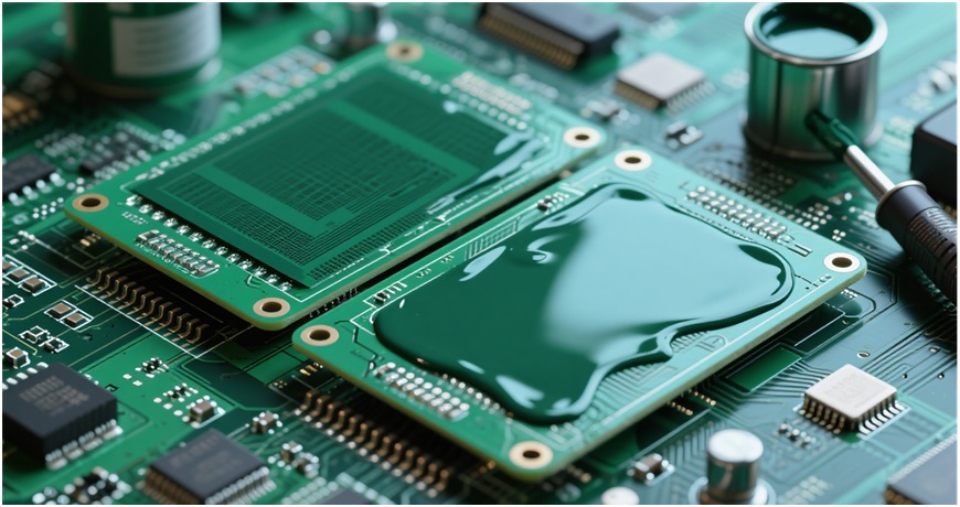
LPSM overlay on PCB board
Performance Characteristics
1. High resolution: It can achieve precise solder mask coverage between fine circuits and small solder pads, meeting the manufacturing needs of high-density interconnect (HDI) PCBs, such as solder mask processing in the packaging area of fine pitch BGA (ball grid array) on mobile phone motherboards.
2. Rich colors: Common colors include green, blue, black, red, etc., which can be customized according to customer needs. Among them, green has become the most widely used color due to its good UV absorption characteristics and high visual comfort.
3. Moderate cost: Compared to some high-end solder mask types, the material cost and production process cost of liquid photosensitive solder mask ink are relatively balanced, which has a cost advantage in large-scale production.
Application scenarios
Widely used in PCB manufacturing of various electronic products, especially in fields with high requirements for circuit accuracy and reliability, such as consumer electronics (mobile phones, tablets, laptops), communication equipment (base stations, routers), industrial control, etc.
Dry Film Solder Mask (DFSM)
Material Properties
Composed of a polyester film carrier, a photosensitive solder mask layer in the middle, and isolation paper, it is in the form of a solid film. The main components of photosensitive solder mask adhesive are similar to liquid photosensitive solder mask ink, but in different forms.

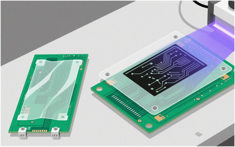
DFSM
Manufacturing Process
1. Film sticking: Using vacuum laminating equipment, dry film solder resist is tightly adhered to the cleaned PCB surface, removing bubbles between the film and the board to ensure good adhesion.
2. Exposure: Similar to the exposure principle of liquid photosensitive solder mask ink, align the patterned film with the PCB with a dry film attached, and perform ultraviolet exposure to solidify the photosensitive components in the dry film.
3. Development: Use a specialized developer to dissolve the dry film of the unexposed area, forming the desired solder mask pattern.
4. Curing: Usually requires thermal curing treatment to further enhance the performance of the solder mask layer.
Performance Characteristics
1. Good thickness uniformity: The dry film thickness can be precisely controlled, generally between 0.05-0.2mm, providing uniform and consistent protection for PCBs, especially suitable for PCBs with high surface flatness requirements, such as circuit boards with fine components.
2. High resolution: It can achieve solder mask for ultra-fine spacing lines and performs well in high-density PCB manufacturing. It can meet strict circuit design requirements for some high-end electronic products, such as high-end server motherboards and aerospace electronic equipment PCBs.
3. Strong chemical resistance: The cured dry film solder mask layer has good resistance to common chemical reagents and can effectively protect the PCB in complex environments.
Application scenarios
Mainly used in fields that require high performance and quality of PCBs, such as aerospace, military defense, high-end medical equipment, etc. These fields have strict requirements for the reliability and stability of electronic devices, and dry film photosensitive solder resist can meet their strict manufacturing standards.
UV Curable Solder Mask
Material Properties
Mainly composed of oligomers such as acrylic esters, combined with photoinitiators, active diluents, and pigments. Sensitive to ultraviolet radiation, it can quickly undergo polymerization reaction and solidify into a film under ultraviolet irradiation.
Manufacturing Process
1. Coating: UV cured solder mask ink is applied to the surface of PCB by spraying, screen printing and other methods.
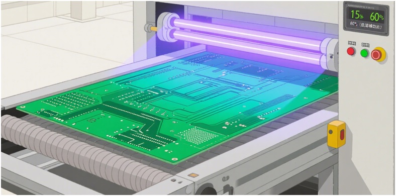
2. UV curing: Place the coated PCB directly under UV irradiation equipment to complete the curing process in a short time (a few seconds to tens of seconds), without the need for high-temperature baking or only low-temperature assisted curing.

UV curing solder mask ink curing process
Performance Characteristics
1. Fast curing speed: greatly improves production efficiency, suitable for large-scale and rapid production scenarios, and can effectively shorten the PCB manufacturing cycle.
2. Energy saving: Compared to thermosetting solder mask, it does not require high temperature heating, reduces energy consumption, and conforms to the concept of green manufacturing.
3. Low thermal impact on the substrate: Especially suitable for temperature sensitive PCB substrates, such as flexible circuit boards (FPCs), it can avoid problems such as substrate deformation and performance degradation caused by high temperatures.
Application scenarios
Commonly used in the manufacturing of flexible PCBs in consumer electronics, such as mobile phone screen cables and flexible circuit boards for wearable devices. At the same time, it is widely used in some ordinary PCB manufacturing that requires extremely high production efficiency, such as simple home appliance control boards, toy circuit boards, etc.
Solvent based Solder Mask
Material Properties
Organic solvents (such as toluene, xylene, etc.) are used as diluents to mix and dissolve synthetic resins (such as phenolic resins, alkyd resins), pigments, fillers, etc. Film formation through solvent evaporation and thermal curing.
Manufacturing Process
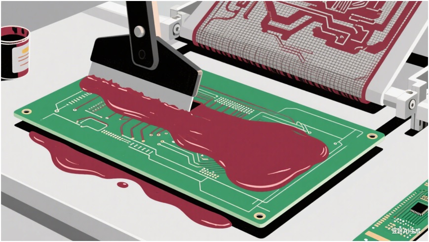
1. Screen printing: Using screen printing technology, solvent based solder mask ink is printed onto the surface of PCB through screen printing to form the desired pattern.
2. Solvent evaporation: After printing, place the PCB in a ventilated environment to allow the organic solvents in the ink to naturally evaporate and dry initially.
3. Thermal curing: After baking at a certain temperature (usually 120-150 ℃), the ink is completely cured.

Screen printing brush
Performance Characteristics
1. Simple process: relying on screen printing, with low equipment requirements and relatively easy operation, suitable for the production of small batches and low precision PCBs.
2. Low cost: Both material and manufacturing costs are relatively low, which gives it an advantage in some cost sensitive and low performance applications.
Application scenarios
Mainly used for PCB manufacturing of toys, simple household appliances (such as electric fans, desk lamp control boards), low-end electronic gifts and other products, these products have relatively low requirements for PCB accuracy and performance, and pay more attention to cost control.
Solder mask differences classified by color
In addition to being classified by material and curing method, solder mask layers are often distinguished by color, and different colors also have differences in certain properties and applications.
1. Green: The most common and cost-effective option. Green pigments (such as phthalocyanine green) have good UV absorption properties and do not affect the photosensitive curing process. In PCB production and maintenance, the contrast between green and copper foil lines is moderate, making it easy to observe and operate.
2. Black: It has good light shielding properties, which can reduce the interference of light on the internal components of the PCB. If applied in circuit boards with many light sensitive components, it can improve equipment stability. At the same time, the black solder mask layer gives the PCB a more technological appearance and is commonly used in high-end consumer electronics, such as high-end mobile phone and tablet motherboards. However, when repairing black, due to its dark color, it is relatively difficult to observe the circuit and requires the use of strong light equipment.
3. Blue/Red: Mostly used to meet customers' personalized needs or to distinguish different functional modules of PCBs, with performance similar to green solder mask layers, commonly used in some specific brand products or industry equipment to highlight product features.
4. White: mainly used in situations where reflection is required, such as the PCB of LED lighting products. The white solder mask layer can reflect the light emitted by the LED, improve the luminous efficiency, and enhance the lighting effect. But the white solder mask has poor dirt resistance and is prone to yellowing after long-term use or in harsh environments.
5. Transparent/Translucent: Used for special needs, such as test boards that require observation of the internal structure of PCBs, or in PCBs that require backlight display, with high requirements for the transmittance of solder mask materials.
Special function solder mask type
1. High temperature resistant solder resist: using special high-temperature resistant resins such as polyimide, modified epoxy resin, etc. Capable of withstanding high temperatures above 260 ℃, meeting the PCB manufacturing needs in lead-free soldering (soldering temperature is usually between 240-260 ℃) and high-temperature environments such as automotive electronics and industrial control, ensuring that the solder mask does not peel off or bubble under high temperature conditions, and continuously protecting the PCB.
2. Flexible solder resist: designed specifically for flexible PCBs, the material has good flexibility and bending resistance. During the repeated bending process of flexible circuit boards, the solder mask layer can remain intact without cracking or peeling, ensuring the electrical connection stability of the circuit. It is widely used in flexible circuit boards for wearable devices, foldable phones, and other products.
3. Lead free compatible solder resist: With the increasing environmental requirements, lead-free soldering is gradually becoming popular. Lead free compatible solder resist has been developed based on the characteristics of lead-free soldering processes. It can adapt well to lead-free solder during high-temperature soldering and has excellent solder resistance. It can withstand multiple high-temperature impacts of lead-free soldering, ensuring reliable solder joint quality. It is widely used in the manufacturing of electronic product PCBs that meet environmental standards.
4. Low surface energy solder resist: Its surface energy is low and it has hydrophobic and oleophobic properties. It can reduce the adhesion of dust and water vapor on the surface of PCB, reduce the risks of short circuit and corrosion caused by the accumulation of pollutants, and improve the reliability of PCB in harsh environments (such as outdoor and humid environments). It is commonly used in outdoor communication equipment, marine electronic equipment, and other PCBs.
In summary, PCB solder mask types are diverse and rich, each with its unique material characteristics, manufacturing processes, performance advantages, and applicable scenarios. In the actual PCB design and manufacturing process, it is necessary to comprehensively consider factors such as the application field, performance requirements, and cost budget of the product, and choose the appropriate solder mask type to ensure the quality and reliability of the PCB and meet the constantly developing needs of electronic products.