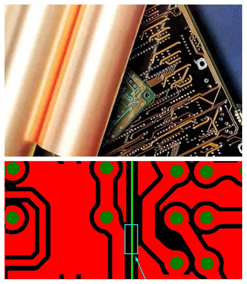
PCB copper-clad: The area filled with copper in the PCB layer. This layer can be the top, bottom, or any interior of a PCB stack, and PCB copper-clad can be used as a ground, reference, or to isolate specific components or circuits from the rest of the elements in this layer.
The function of PCB copper coating
Grounding on double-layer PCB
Both layers are used for signals and there is no ground plane. For these circuit boards, grounding copper can greatly facilitate efficient wiring by providing a central ground.
EMI shielding
For a good multi-layer design, it is desirable to have a ground plane between two signal layers to minimize noise to the greatest extent possible. If there is an internal signal layer next to the surface signal layer, grounding copper can help reduce noise by adding shielding.
Heat dissipation
Grounding copper can also be used to absorb heat from high-power components, and then excess heat can be removed from the circuit board using heat dissipation holes.
Copper balance
PCB grounding copper coating can also be achieved during PCB assembly by balancing the amount of copper on both sides of the circuit board to achieve contract manufacturer (CM), reducing the possibility of warping during reflow process. In this case, a cross copper grid may be a better alternative to solid copper grounded copper cladding.
Large circuit path
Adding surface grounding copper can provide a shorter return path for high current devices, such as switch converters, instead of connecting longer wires to the ground plane.
Easy to manufacture PCB
Provide uniform copper distribution on one layer, improve etching and electroplating processes, and reduce the amount of etching solution used in PCB manufacturing (reducing costs).
RF and microwave design
Grounding copper cladding contains electromagnetic (EM) radiation in localized areas, thereby reducing stray coupling, radiation, and dispersion.
Digital Design
The ground plane improves immunity, enhances grounding uniformity, and improves low inductance current paths.
Ground uniformity and improve the low inductance current path.

PCB Copper Coating Techniques
If there are many ground points on the PCB, such as SGND, AGND, GND, etc., they need to be independently copper-clad based on the different positions of the PCB surface, using the most important "ground" as a reference. It goes without saying that digital ground and analog ground should be separately copper-clad. At the same time, before copper-clad, the corresponding power lines should be thickened: 5.0V, 3.3V, etc., thus forming multiple different shaped multi deformation structures.
For single point connections in different locations, the method is to connect them through 0-ohm resistors, magnetic beads, or inductors.
The copper coating near the crystal oscillator is used as a high-frequency emission source in the circuit. The method is to wrap copper around the crystal oscillator and then ground the outer shell of the crystal oscillator separately
The island (dead zone) problem, if you think it's too big, it doesn't take much effort to define a ground via and add it.
At the beginning of wiring, the ground wire should be treated equally. When routing, the ground wire should be properly placed and cannot be eliminated by adding vias after copper coating, as this effect is not good.
It is best not to have sharp corners on the board (=180 degrees), because from an electromagnetic perspective, this constitutes a transmitting antenna! For others, whether it is large or small will always have an impact. I suggest using rounded edgesDo not lay copper in the open area of the wiring in the middle layer of the multi-layer board. Because it's difficult for you to achieve a good grounding for this copper coating.
The metal inside the equipment, such as metal heat sinks, metal reinforcement bars, etc., must be well grounded.
The heat dissipation metal block of the three terminal voltage regulator must be well grounded. The grounding isolation strip near the crystal oscillator must be well grounded. In short, if the grounding issue on the PCB is properly addressed, the benefits outweigh the drawbacks. It can reduce the return area of signal lines and minimize electromagnetic interference to external signals.