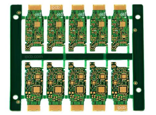
HDI PCB stands for High Density Interconnect PCB. HDI PCB manufacturing is currently one of the fastest growing areas of the circuit board industry.
From the first 32-bit computer introduced by HP in 1985, to large-scale client servers with 36 sequences of layered multilayer printed boards and stacked microvias, HDI/microvia technology is undoubtedly the PCB architecture of the future. Larger ASICs and FPGs with smaller device spacing and more I/O pins, as well as embedded passive devices with shorter rise times and higher frequencies, and all of which require smaller PCB feature sizes, are driving the strong demand for HDI/Microvias.
Advantages of HDI PCB
Stable production, low defective rate, high yield rate, and high precision for HDI daily operation. The required number of PCB boards per day achieves the required production volume. As mentioned earlier, the relative quantity of the required output should be considered in the accuracy requirements. To achieve the required throughput, high throughput is achieved through automatic control.
Low cost, this is a major requirement for any volume manufacturer. Early LDI models may need to replace a more sensitive dry film with a more sensitive dry film to achieve faster imaging speeds. Or the dry film may be changed to a different wavelength, depending on the light source used in the LDI mode. In all of these cases, the new dry film is typically more expensive than the traditional dry film used by the manufacturer.
Good compatibility with existing processes and production methods. Mass production processes and methods are often carefully specified to meet mass production requirements. The introduction of any new imaging method should minimise changes to existing methods. This includes minimal changes to the dry film used, the ability to expose layers of soldermask, traceability features required for volume production, etc.
Optical Module HDI PCB, take a look at this type of HDI PCB circuit board.

Optical Module HDI PCB
Optical module (optical module) consists of optoelectronic devices, functional circuits and optical interfaces, etc. The optoelectronic device consists of two parts: the transmitting and receiving parts.
Simply put, the role of the optical module is to convert electrical signals into optical signals at the transmitting end, and then convert the optical signals into electrical signals at the receiving end after transmission through optical fibres.
The optical module includes an optical module housing, a fiber optic connector, a transmitter-side optical component, a receiver-side optical component, and a printed circuit board, wherein: said transmitter-side optical component, said receiver-side optical component, and said printed circuit board are set up inside said optical module housing; said transmitter-side optical component and said receiver-side optical component are optically coupled with said fiber optic connector, and electrically coupled with said printed circuit board; said printed circuit board said printed circuit board forming a horizontal arrangement inside said optical module housing; said transmitting end optical component and said receiving end optical component forming a stacked arrangement in a direction perpendicular to said printed circuit board.
The optical module includes the following types:
1. 10Gbs optical modules (XFP, SFP+) - compact 10Gb/s optical transceiver modules for applications in continuous optical communications (metropolitan area networks, Ethernet, optical fibre pathways).
2.1x9 duplex SC ST connector optical module.
3.RJ45 port compact pluggable module
4.Point-to-Point Bidirectional Optical Module (P-to-P FTTH application)
5.Gigabit Ethernet Interface Converter (GBIC) Module
6.Passive Optical Network PON (G-PON, GE-PON) Optical Module
7.Small Form Factor Pluggable Optical Module (SFP, SFF)