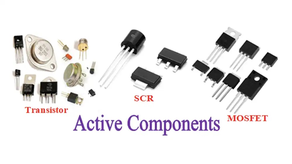
Active components are fundamental building blocks in modern electronic systems. They are commonly defined as electronic components that require an external power source to operate and are capable of controlling, amplifying, or generating electrical signals.
Typical active components include integrated circuits (ICs), transistors, MOSFETs, diodes, voltage regulators, microcontrollers, and power management devices. While this functional definition is widely accepted, it represents only a surface-level understanding. From an engineering and manufacturing perspective, active components introduce a distinct set of challenges that go far beyond circuit functionality.
To fully understand their role in PCBA, active components must be examined not only as electrical elements, but as structurally complex, process-sensitive devices whose behavior is strongly influenced by assembly conditions.
1. Fundamental Characteristics of Active Components
The defining characteristic of an active component is its dependence on energy. Unlike passive components, which respond predictably to applied signals, active components require biasing, power sequencing, and defined operating conditions to function correctly.
Internally, active components contain semiconductor structures such as silicon dies, gate oxides, diffusion layers, metallization networks, and bonding interfaces. These structures operate within narrow electrical and thermal margins and are sensitive to mechanical and environmental stress.
This internal complexity is the primary reason why active components behave differently from passives during manufacturing and operation. They are not merely conductive elements; they are functional systems encapsulated within a package.
2. Packaging as an Inherent Requirement
Active components cannot exist in an unpackaged form within a PCB assembly. The semiconductor die must be protected, electrically connected, and mechanically supported, which makes packaging unavoidable.
Common package types include QFN, BGA, LGA, SOP, and various power packages. Each package introduces multiple materials with different coefficients of thermal expansion, such as silicon, mold compound, lead frames, and solder.
During reflow soldering, these materials expand and contract at different rates, creating internal stresses. Even when external solder joints appear acceptable, stress may already be present inside the package. This is a structural characteristic of active components, not a process defect.
As a result, package-related risks are intrinsic to active devices and must be considered during assembly planning.
3. Moisture Sensitivity and Latent Damage
Most plastic-packaged active components absorb moisture from the environment. When exposed to high temperatures during reflow, trapped moisture expands rapidly, potentially causing internal damage.
Typical moisture-related failure mechanisms include:
Internal delamination
Die attach separation
Micro-cracking within the package
Degradation of internal metallization
In many cases, these failures are not immediately visible. The component may still function and pass standard electrical tests. However, its long-term reliability is compromised.
This is why MSL (Moisture Sensitivity Level) control is a critical requirement for active components. Floor life tracking, dry storage, and baking procedures are not optional best practices—they are necessary controls dictated by the nature of active devices.
4. Assembly Stress and Reduced Operating Margin
Active components are particularly sensitive to assembly-induced stress, including thermal stress, mechanical stress, and solder joint deformation.
Unlike passive components, which typically fail in a binary manner (open or short), active components often experience partial degradation. Examples include weakened gate oxides, bond wire fatigue, or die-level micro-cracks.
These defects reduce the operating margin of the device without causing immediate failure. The component may continue to operate under light loads but fail under elevated temperature, higher current, or long-term use.
This explains why active-component-related issues often appear as intermittent or delayed failures rather than immediate assembly defects.

5. Thermal Behavior as a Functional Constraint
For many active components, thermal performance directly determines functionality. Power devices, processors, and regulators must dissipate heat efficiently to maintain safe junction temperatures.
In such cases, solder joints beneath the component serve multiple purposes:
Electrical interconnection
Mechanical support
Thermal conduction
Assembly factors such as solder voiding, thermal pad design, via-in-pad implementation, and copper plane connectivity all influence heat dissipation efficiency.
Minor variations in assembly quality can result in measurable temperature differences at the silicon junction level, accelerating aging and reducing device lifetime.
Passive components rarely exhibit this degree of thermal dependency.
6. Power Dependence and Testing Limitations
Another defining trait of active components is that their defects are often condition-dependent. Many failure mechanisms only become apparent when the component is powered and operating under realistic conditions.
A marginally damaged device may pass static tests but fail during:
Load transients
High-speed switching
Power cycling
Thermal cycling
This limitation highlights the importance of functional testing strategies that reflect actual operating conditions, rather than relying solely on basic electrical verification.
7. Engineering Implications for PCBA Manufacturing
Because active components dominate both risk and complexity, they should be the primary focus of DFM and process control efforts.
Key engineering practices include:
Package-specific land pattern and stencil optimization
Strict MSL handling and storage control
X-ray inspection for hidden solder joints
Thermal and power cycling during validation
Defined acceptance criteria for voiding and solder integrity
Treating active components as ordinary SMT parts often results in assemblies that meet formal inspection criteria but lack sufficient reliability margin.
Conclusion
Active components are best understood not simply as functional circuit elements, but as highly sensitive systems embedded within a PCB assembly. Their internal complexity, reliance on packaging, and sensitivity to thermal, mechanical, and electrical stress make them the primary drivers of manufacturing risk and long-term reliability.
A PCBA process that is optimized around active components—rather than treating them as interchangeable parts—will consistently achieve higher yield, lower field failure rates, and more robust product performance.