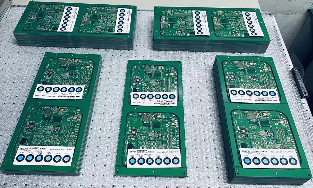
Double sided pcb board is a very important PCB in the circuit board, the market has a double-sided pcb board metal-based PCB, Hi-Tg heavy copper foil PCB, flat meandering double-sided circuit boards, high-frequency PCB, mixed dielectric base high-frequency double-sided pcb, etc., which is suitable for a wide range of high-tech industries such as: telecommunications, power supply, computers, industrial control, digital products, scientific and educational equipment, medical equipment, automotive It is suitable for a wide range of high-tech industries such as: telecommunications, power supply, computers, industrial control, digital products, scientific and educational instruments, medical equipment, automotive, aerospace defense, etc.
Advantages of double sided circuit boards
Double-sided PCBs make it relatively easy to add conductor paths to the board, which means you will have a PCB that better suits your needs.
Since they are conductive on both sides, a large number of ICs and components can be readily assembled.
Compared to single-sided boards, there is an extra layer so that you can add as many components as you need.
Double sided PCBs have more space for flexible design, which means you are more likely to have a PCB that suits your requirements.
Double sided PCB boards are ideal for demanding applications and advanced electronics.
If required, the size of the board can be reduced as double-sided can be used.
Double sided PCB boards can be cost effective as you may only need to use one board to meet your design and utilization requirements.
Dual-sided PCBs can be used in many different applications and electronic products. In other words, they are ideal for a wide range of industries.
Disadvantages of double-sided PCBs
Duplex PCBs are not ideal for conducting high currents because the copper wires are heated. We are aware of this and ensure that all PCBs are of high quality and are not damaged.
There is a risk of overheating when soldering this type of PCB. However, we are experienced PCB manufacturing specialists and we know how to minimize the risk.

double sided circuit board
Double sided circuit boards are usually made of epoxy glass cloth laminated with copper foil. It is mainly used in communication electronic equipment, advanced instrumentation and electronic computers with high performance requirements.
The production process of double-sided PCB is generally divided into several kinds of process wire method,plug hole method, masking method and graphic plating an etching method.
Double-sided PCB prototyping, the most commonly used process. At the same time, rosin technology,OSP technology, gold plating, gold plating, silver plating these processes, in the double-sided circuit boards are also applicable.
Spray tin process: good appearance,silver-white pads, easy to tin the pads, easy soldering,low price.
Soldering process: Stable quality, usually used in the case of bonded ICs.
The difference between double-sided PCB and single-sided PCB is that the single-sided circuit is only on one side of the PCB,while the double-sided PCB circuit can be on both sides of the PCB, with a hole in the middle to connect the two sides of the PCB circuit.
Parameters of double-sided PCBs.The production of double-sided PCBs is different from that of single-sided PCBs, except that there is an additional copper sinking process,that is, the process of connecting the wires on both sides of the board.
Double-sided tinplate/immersed gold plate production process
Open->Drilling->Embossing->Wiring->Patterned->Etching->Solder Resist->Writing->Spraying tin (or gold-immersed)-Causeway Edge->V-cutting (some boards don't need it)->Flight Test->Vacuum Packing.
Double-sided gold-plated board production process
Uncutting->Drilling->Copper sinking->Wiring->Patterned->Gold plating->Etching->Soldering->Character->Causeway->V-cutting->Flight test->Vacuum packing.
Double sided PCB Characteristics
The difference between single-sided and double-sided boards is the number of copper layers.Duplex boards have copper on both sides of the board and can be connected through holes. However, since there is only one layer of copper on one side, it can only be used for simple circuits and the holes punched out can only be used for insert connections. The technological requirement of double-sided circuit boards is that the density of wiring becomes larger and the aperture diameter becomes smaller, and the aperture diameter of metallized holes becomes smaller and smaller. The quality of the metallized holes on which the interconnection between layers depends is directly related to the reliability of the board.As the aperture shrinks, debris that does not affect the larger aperture, such as brush chips, once left in the small holes, will make the chemical copper plating and electroplating lose its effect, appearing no copper holes and become holes. Fatal metallization killer.
Double-sided circuit boards have wires on both sides.However, in order to use wires on both sides, there must be a proper circuit connection between the two sides. This “bridge” between circuits is called a via. Through-holes are small holes filled or coated with metal on the PCB that can be connected to the wires on both sides. Because double-sided PCBs are twice the size of single-sided boards, and because the traces can be staggered (wrapped around to the other side), they are more suitable for more complex circuits than single-sided boards.