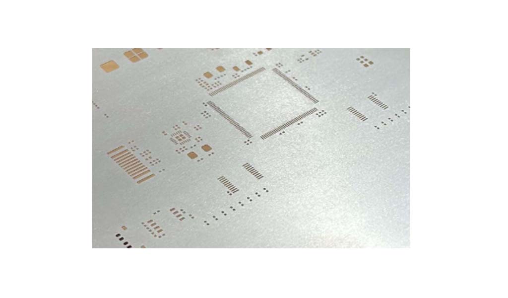
Stencil PCB is a key tool in the manufacturing process of printed circuit boards for surface mount technology. It is a metal or plastic sheet with precise openings, usually made using laser cutting or chemical etching technology. The openings for placing solder paste on the PCB are precisely cut out. These openings correspond to the pad positions on the PCB and are used to accurately apply solder paste or adhesive to the specified positions during the PCB manufacturing process. When the Stencil is placed on the PCB board, the solder paste is applied to the pads of the PCB through these openings to prepare for the soldering of the components.
Function:
Precisely dispense solder paste: With Stencil, solder paste can be accurately dispensed to the pads of the PCB, ensuring that each component has the right amount of solder paste for soldering.
Improve production efficiency: Stencil PCB can greatly improve the speed and accuracy of solder paste printing, suitable for mass production.
Reduce errors: Through standardized templates, errors caused by manual operation can be reduced and uniform solder paste coating can be ensured.
Advantages:
High precision: Stencil PCB can provide extremely high solder paste coating accuracy, ensuring good contact between components and PCB pads.
High efficiency: Suitable for mass production, can significantly improve production speed and consistency.
Consistency: Each PCB can get the same solder paste coating, ensuring consistency in mass production.
Improve product quality: The use of stencil helps to reduce undesirable phenomena in the welding process, such as poor welding, welding offset, etc., thereby improving the reliability and stability of welding and reducing product quality problems caused by welding problems.
Disadvantages:
High cost: Precision equipment and materials are required to make high-quality Stencils, and the initial cost is high.
Low flexibility: Stencil PCB is suitable for mass production, and it is difficult to modify once the design is completed. If the design changes frequently, the cost of use will increase significantly.
Poor adaptability: For small batches or prototype development, it is not applicable due to the high time and cost of changing the stencil.
In summary, Stencil plays an important role in mass production, but there are certain limitations in flexibility and cost.

There are some key points to note when developing or ordering a PCB stencil:
Thickness of the stainless steel sheet: The precise thickness of the stencil sheet ensures that the required amount of solder paste is released through the openings. The thickness of the sheet and the aperture size are important factors affecting the amount of solder paste deposited on the board, as extra solder deposition can lead to solder bridging. On the other hand, less solder deposition can also create weak solder joints, which can affect the functionality of the final PCB board.
Aperture size of the openings created: To avoid soldering defects such as bridging and solder beads, the stencil openings are designed slightly smaller than the PCB pad size. After solder deposition, when the stencil is removed from the board, the solder paste may transfer to the PCB or stick to the stencil's hole walls. The area of the PCB pad should always be larger than two-thirds of the area of the inside of the stencil's hole walls to avoid this problem.
Stencil material: The stencil material also affects its ability to deliver solder paste from the openings/apertures to the PCB pads. Stainless steel is the material commonly used for stencils.
Stencil Alignment: In order to perfectly print solder paste on PCB pads, registration marks called "fiducial marks" are added to both the PCB and the stencil. These fiducial marks ensure good alignment between the PCB and the stencil.
Stencil is widely used in the manufacture of various electronic products, including but not limited to mobile phones, computers, LED displays, automotive electronics, industrial control equipment, medical equipment and other fields. In these fields, Stencil PCB is a key tool to achieve precise connection between electronic components and PCBs.