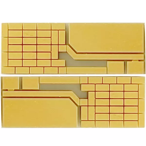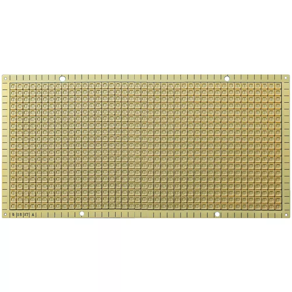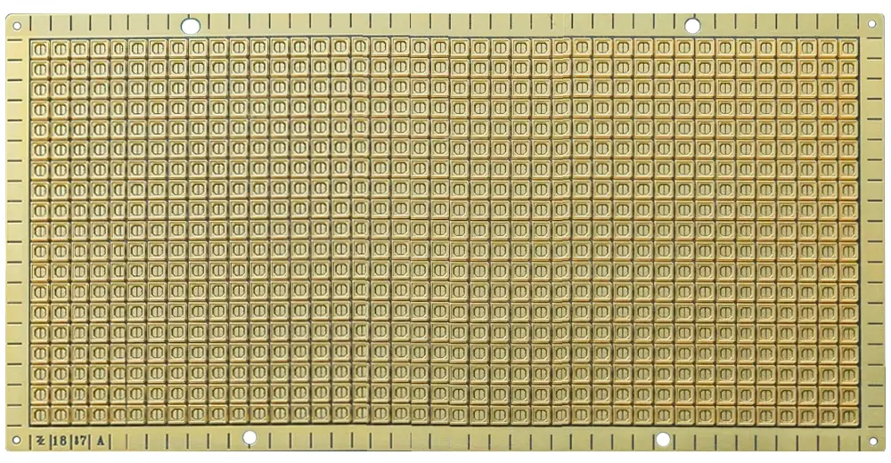

Substrate type: Aluminum Nitride Ceramic
Substrate thickness: 0.3-2.0mm
Conductive layer: copper, nickel, gold
Metal layer thickness: 35-400μm
Surface treatment: Nickel gold
Metal: 1L
Conductive hole: 0.2mm conductive hole
Line width: 0.1mm
Application: High-power LED
Aluminum nitride (AIN) ceramic PCB is an advanced ceramic material with aluminum nitride as the main crystal phase. Due to its high thermal conductivity, non toxicity, good corrosion resistance, high temperature resistance, and excellent electrical insulation, it plays an irreplaceable role in the heat dissipation and packaging applications of high-density, high-power, and high-speed integrated circuits. Its thermal expansion coefficient matched with silicon further consolidates its application position in the semiconductor industry, making it an ideal material choice for manufacturing high-performance electronic devices.
The development prospects of AIN ceramic PCB are positive and promising.
1. Aluminum nitride ceramics have become an ideal choice for the new generation of heat dissipation substrates and electronic device packaging due to their excellent thermal conductivity, thermal expansion coefficient matched with silicon, high mechanical strength, and stable chemical properties. This has led to its widespread application in high-performance electronic devices, such as the packaging of hybrid power switches, microwave vacuum tube packaging housings, and large-scale integrated circuit substrates.
2. With the rapid development of 5G communication, new energy vehicles, and semiconductor industries, the demand for high-performance electronic materials is increasingly strong. The demand for aluminum nitride ceramic substrates in the fields of heat dissipation and electronic packaging is expected to continue to rise, especially in high-end electronic products and power electronic equipment.
3. The continuous advancement of technology will improve the production efficiency and product quality of aluminum nitride ceramic substrates, reduce production costs, and further promote industry development.

AIN ceramic PCB
The development history of AIN ceramic PCB industry is far away. Initially, aluminum nitride was developed by F Birgeler and A Geuhter discovered in 1862 that aluminum nitride was not widely used for a long time due to its covalent properties, such as low self diffusion coefficient and high melting point, and only existed as a nitrogen fixing agent in fertilizers.
It was not until the 1950s, when breakthroughs were made in the preparation process of aluminum nitride ceramics, that they were first used as refractory materials in the melting of specific metals. With the deepening of scientific research, especially since the 1970s, the preparation technology of AIN PCB has gradually matured. The excellent thermal conductivity, high insulation performance, and chemical stability of AIN PCB have also made it widely used in multiple fields, especially in high-tech fields such as 5G communication, semiconductor, aerospace, and automotive electronics.
The development of the AIN PCB industry has also followed this trajectory. With the deepening of research on aluminum nitride ceramic substrates by scientific research institutions and universities, significant progress has been made in technology.
Due to the enormous potential of the aluminum nitride ceramic PCB market, iPCB has increased investment to drive rapid industry development. Nowadays, AIN PCB products have formed a competitive brand.
The development of AIN PCB still faces challenges in various aspects such as technological innovation capability, cost control, and market competition. In order to promote the sustained and healthy development of the industry, enterprises and research institutions need to continue to increase investment, strengthen cooperation, jointly overcome technical difficulties, improve product quality and reduce costs, in order to better meet market demand. With the continuous advancement of technology and the expansion of the market, the development prospects of the AIN PCB will be even broader.
Substrate type: Aluminum Nitride Ceramic
Substrate thickness: 0.3-2.0mm
Conductive layer: copper, nickel, gold
Metal layer thickness: 35-400μm
Surface treatment: Nickel gold
Metal: 1L
Conductive hole: 0.2mm conductive hole
Line width: 0.1mm
Application: High-power LED
iPCB Circuit provides support for PCB design, PCB technology, and PCBA assembly. You can request technical consultation or quotation for PCB and PCBA here, please contact email: sales@ipcb.com
We will respond very quickly.