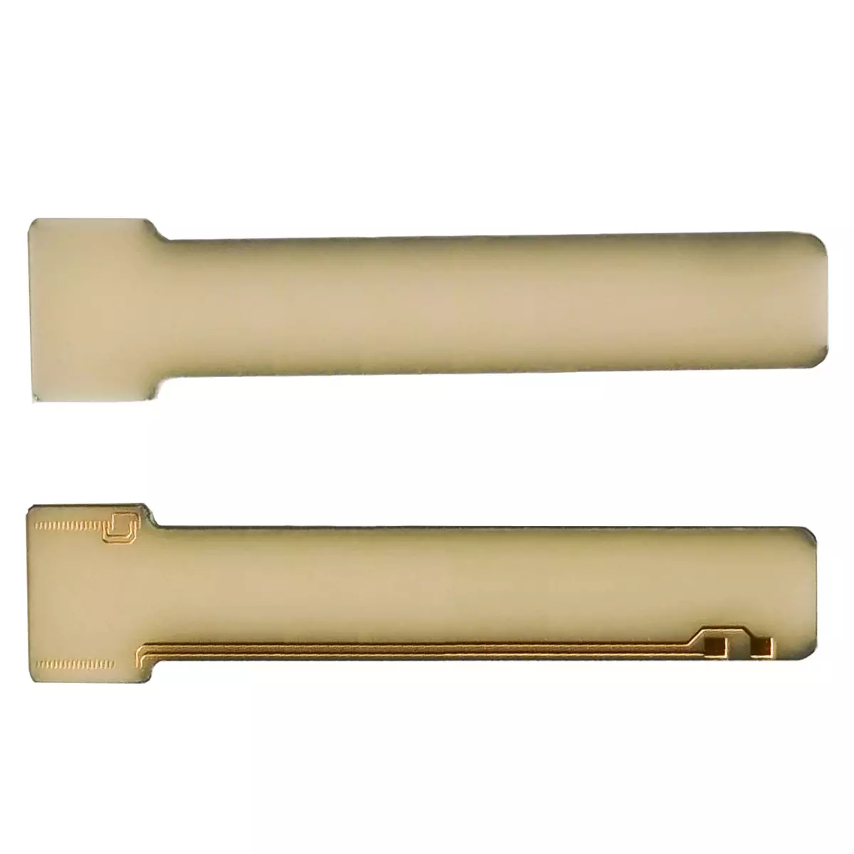
Substrate type: AIN Ceramic
Substrate thickness: 0.3-3.0mm
Conductive layer: copper, nickel, gold
Metal layer thickness: 35-400μm
Surface treatment: Nickel gold
Metal: 1L
Conductive hole: 0.2mm conductive hole
Line width: 0.1mm
Application: High power component
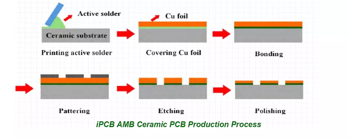
AMB ceramic PCB (Active metal brazing) is a process of tightly soldering copper foil and ceramic sheets using metal brazing materials containing a small amount of active elements. The small amount of active elements added to AMB brazing material has high activity, which can improve the wettability of the brazing material to ceramics after melting, allowing the ceramic surface to achieve good welding with metals without the need for metallization.
AMB substrates with copper coating on ceramic surfaces achieved through brazing have higher bonding strength and better reliability compared to DBC ceramic PCB. The ceramics in AMB ceramic PCB are generally Si3N4 ceramics and AlN ceramics, and their thermal conductivity (Si3N4 AMB>80W/m · K, AlN AMB>170 W/m · K) is much higher than that of Al2O3 DBC (24W/m · K). In addition, Si3N4 AMB also has excellent mechanical strength.
The explosive development of new energy vehicles has also brought about a rapid increase in demand for automotive power modules. At the same time, SiC power devices are gradually maturing and beginning to be widely applied, which is also driving the continuous improvement of power density in power modules. Therefore, higher requirements have been put forward for the heat dissipation performance, mechanical strength, and reliability of packaging materials. AMB ceramic PCB, especially Si3N4 AMB ceramic PCB, meet the performance requirements of automotive SiC power modules very well.

AMB ceramic PCB is developed based on DBC technology. At a high temperature of around 800 ℃, AgCu solder containing active elements Ti and Zr wets and reacts at the interface between ceramics and metals, thereby achieving heterogeneous bonding between ceramics and metals.
Due to the high thermal conductivity (>90W/mK) of AMB silicon nitride substrate, very thick copper metal (up to 0.8mm thickness) can be soldered onto relatively thin silicon nitride ceramics, resulting in high current carrying capacity. And the thermal expansion coefficient of silicon nitride ceramic substrate is close to that of the third-generation semiconductor substrate SiC crystal, making it more stable to match with SiC crystal materials. Therefore, it has become the preferred material for SiC semiconductor thermal conductive substrate, especially indispensable in high-end new energy vehicles above 800V.
AMB technology has achieved the overlay of aluminum nitride and silicon nitride ceramics with copper sheets. Compared with DBC liners, it has better thermal conductivity, copper layer adhesion, reliability, etc., which can greatly improve the reliability of ceramic liners. It is more suitable for high-power and high current application scenarios and has gradually become the main application type of mid to high end IGBT module heat dissipation circuit boards, widely used in the fields of automobiles, aerospace, rail transit, industrial power grids, etc.

AMB ceramic PCB
Compared with traditional ceramic PCB, AMB ceramic PCB rely on chemical reactions between ceramics and active metal solder paste at high temperatures to achieve bonding, resulting in higher bonding strength and better reliability. They are highly suitable for connectors or scenarios with high current carrying and heat dissipation requirements. Especially for power electronics and high-power electronic modules with strict performance requirements such as new energy vehicles, rail transit, wind power generation, photovoltaics, and 5G communication, there is a huge demand for AMB ceramic PCB.
Substrate type: AIN Ceramic
Substrate thickness: 0.3-3.0mm
Conductive layer: copper, nickel, gold
Metal layer thickness: 35-400μm
Surface treatment: Nickel gold
Metal: 1L
Conductive hole: 0.2mm conductive hole
Line width: 0.1mm
Application: High power component
iPCB Circuit provides support for PCB design, PCB technology, and PCBA assembly. You can request technical consultation or quotation for PCB and PCBA here, please contact email: sales@ipcb.com
We will respond very quickly.