Reliability of electronic products is PCB components and PCB as a carrier of various components and circuit signal transmission hub, has become the most important and critical components of electronic products, PCB quality and reliability level will determine the quality and reliability of the entire equipment.
1.PCB blistering
IPC-A-610 standard has given a clear definition of the layered blistering.
PCB blistering: a form of delamination that manifests itself as localised expansion and separation between any layers of a laminated substrate, or between a substrate and a conductive film or protective layer.
PCB Delamination: The separation between layers of a substrate, between a substrate and a conductive foil, or between other layers within a PCB.
Specifically refer to the following figure, PCB delamination on the surface of the board is characterised by the appearance of ‘whitening’, while the blistering is characterised by the appearance of ‘bulging’.
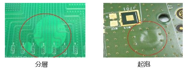
PCB layering blistering diagram
1.1 Characteristics of PCB delamination blistering key factor diagrams
The following analyses are based on the failure cases in the factory, and also collected from the field experience of PCB factories and the analyses data of the industry peers.
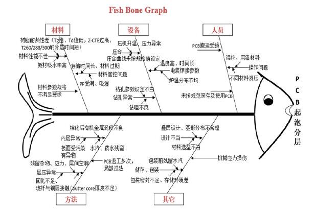
PCB layered blistering fishbone diagram
1.2 Failure Analysis Procedure for PCB Delamination Blistering
Special emphasis, unless the PCB is confirmed to be damp, it is not recommended to do unnecessary baking action on the PCB.Baking itself is a ‘double-edged sword’,on the one hand, can indeed play a role in dehumidification, but it produces a lot of negative effects, if the baking temperature, time set improperly will accelerate the risk of blistering of its delamination,and at the same time on the PCB plating layer is also a test. Baking will accelerate the oxidation of the plating layer affecting its weldability, especially the OSP surface treatment needs to be handled with care.
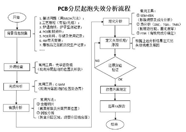
Failure analysis process of PCB delamination blistering
2.PCB internal short defects
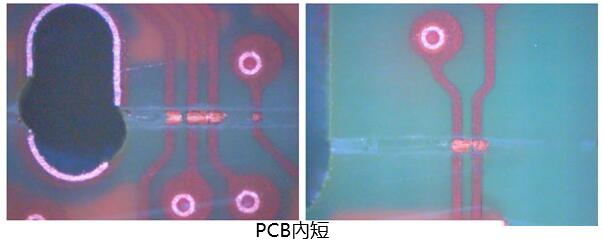
Internal short, i.e. PCB electrical test found in the inner layer short circuit.Defects occur in the inner layer of the map to the multi-layer compression process, as shown in the figure below, for the inner short of the photograph of the slice.On the surface, this part of the inner layer system process is very simple,but after actual research,it is found that the causes of internal short are many and varied,and even beyond the inner layer system process,the extent of which is far beyond our imagination.
In order to find out the cause of internal shorting,we must first master the method of analysing internal shorting,in other words,we must find out the location of the short circuit in the inner layer.Since the final product has gone through the process of lamination, solder resist coating, etc.,it is difficult for us to see the location of the internal short circuit at a glance,and then we must analyse it by certain means. The specific analysis process is as follows:
2.1 Electrical test to find the point
For products found to be short-circuited in the electrical test, the locator will find out the location of the short-circuit by means of the locator software and defect coordinates, and then point out the marking on the outer network.
2.2 Network Analysis
Network analysis is performed on the product after the pointing to find the location of the short circuit in the inner layer. We can establish a network on the defect location through the engineering data processing software (e.g. UCAM, GENESIS, etc.) to find out where the inner short is located in the layer and the location.
2.3 Flat grinding slices
Sample the slices at the defect location, and grind the slices flat to the level of the internal short analysed by the network above, it is better not to grind all the PP on the layer where the internal short is located, so as not to destroy the defect state and affect the judgement of the defect.
3.PCB burst board failure
PCB burst board location for slicing observation, found that the core board of copper foil and resin between the development of separation. This interface separation causes from two considerations: First, soldering substrate thermal expansion is too large; Second, the two interfaces themselves weak bond, and the causes of the two weak bond is more complex.
3.1 Coefficient of thermal expansion of the substrate
The coefficient of thermal expansion (Z-CTE) and the percentage of expansion (PTE) of PCB substrate are tested, and the results show that the α 1-CTE of PCB substrate is 54.7 ppm/°C, the α 2-CTE is 288.2 ppm/°C, and the PTE is 3.95%. Referring to IPC-4101C, for FR-4 substrate with Tg less than 150℃,α 1-CTE should be no more than 60 ppm/℃, α 2-CTE should be no more than 300 ppm/℃, and PTE is no more than 4.0%. This indicates that the PCB expansion during soldering is within acceptable limits. The TMA test curve is shown below:
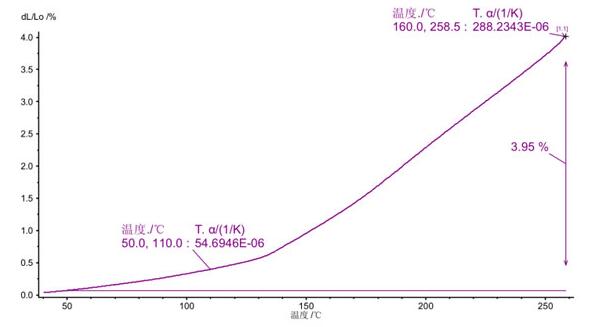
TMA test curves for substrates
3.2 Scanning electron microscope observation
Peel off the bursting plate position, the substrate and copper foil for observation, found that there is no obvious residue of resin on one side of the copper foil,and no contamination between the two, indicating that the resin did not form a good wetting of the copper foil during pressing.A scanning microscope was used to observe the two sides of the stripped foils,and it was found that there were problems with the surface treatment of the copper foils. Comparing the copper foil of the core board of the failed batch and the normal batch,it is found that there is a significant difference between the two.The copper foil of the core board of the normal batch has a higher density of copper tumours on the gross surface and a rougher surface, while the copper foil of the core board of the failed batch has a smaller density of copper foil on the gross surface and a smoother surface, which will reduce the bonding force between the copper foil and the resin.
The above is iPCB's analysis of PCB delamination blistering, internal shortening, exploding boards and other common problems.If you have any related PCB questions,please feel free to contact iPCB.