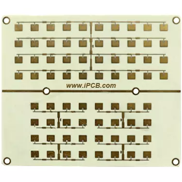
Substrate: Rogers, Taconic, Alron
Material: Teflon, ptfe, Fr-4
Dielectric constant: 2.2-10.2
Base copper thickness: 18um (0.5oz)
Finished copper thickness: 35um (1oz)
Medium thickness: 0.1mm-6.0mm
Finished product thickness: 0.2-6.0mm
Solder mask color: customized
Screen color: customized
Surface treatment: silver, glod
Product application: Communication Antenna PCB
Antenna PCB, also known as antenna circuit board, is an antenna that is directly printed on the PCB. Antenna PCB plays an increasingly important role in modern wireless communication devices, especially in mobile devices, IoT devices, and wireless sensor networks. Due to its compact, lightweight, and low-cost characteristics, it has been widely used.
The design principle of antenna PCB is based on electromagnetic field theory. By arranging specific metal conductor patterns on the PCB board, effective electromagnetic radiation and reception structures can be formed, thereby achieving wireless signal transmission and reception. The performance of antenna PCB is influenced by various factors, including the shape, size, material of the conductor pattern, and the dielectric properties of the PCB board. Therefore, when designing antenna PCB, it is necessary to comprehensively consider these factors to ensure that the performance of the antenna meets practical application requirements.
There are various types of antenna PCB, including dipole antennas, monopole antennas, loop antennas, slot antennas, etc. These antenna forms each have their own advantages and disadvantages, and are suitable for different application scenarios. For example, dipole antennas have good radiation performance and stability, making them suitable for general wireless communication devices; The monopole antenna, on the other hand, has a smaller size and lower cost, making it suitable for miniaturized and low-cost application scenarios.
In practical applications, the design and optimization of antenna PCB is a key task. Designers need to select appropriate antenna forms and parameters based on specific wireless communication standards, device dimensions, performance requirements, and other factors, and conduct detailed simulations and tests. By continuously optimizing antenna design, the performance, stability, and reliability of wireless communication devices can be improved.
In addition to design optimization, the production and installation of antenna PCB are also important tasks. During the production process, it is necessary to ensure the quality of the PCB board, the accuracy and consistency of the conductor pattern, and other factors to ensure the performance of the antenna. When installing, it is necessary to consider the position, direction, impedance matching, and other issues of the antenna to ensure that it can be effectively integrated with other parts of the wireless communication device.
As an important component of modern wireless communication devices, antenna PCB design and application involve knowledge and technology from multiple fields. Through continuous research and innovation, we can expect antenna PCB to play a more important role in the future wireless communication field. At the same time, it is also necessary to pay attention to the problems and challenges that antenna PCB may face in practical applications, such as electromagnetic interference, antenna matching, etc., and take corresponding measures to solve them.
In practical applications, PCB antenna also need to be coordinated with other wireless communication device components, such as RF transceivers, filters, power amplifiers, etc. Therefore, for the design and application of antenna PCB, comprehensive wireless communication knowledge and technical background are required. At the same time, it is also necessary to pay attention to the development trends and market demands of wireless communication technology, constantly innovate, and contribute to the development of the wireless communication field. With the continuous development and progress of wireless communication technology, the continuous advancement of PCB board manufacturing technology and the continuous reduction of costs, antenna PCB will also be applied in more fields.
Antenna PCB
PCB Antenna is used for antennas in wireless communication base stations. Communication base station, abbreviated as BSA, is a complex communication system that requires a large number of various forms of circuit board to achieve different functions. IPCB supplies a variety of communication base station PCB, including phase shifter PCB, slider PCB, array substrate circuit boards, array support PCB, array arm PCB, power divider PCB, parasitic component PCB, isolation PCB, calibration board PCB, antenna PCB, etc.
Unlike PCB used in high-speed base stations, servers, high-speed computers, industry, aerospace, and other fields, single-layer, double-sided, and three-layer designs are more common in communication base station PCB. Although multi-layer is not very common, iPCB still produces and delivers multi-layer antenna circuit boards to end customers, up to 7 layers, for antenna PCB used in 5G scenarios.
Base station antennas can operate in various frequency bands, such as 600MHz, 700MHz, 750MHz, 800MHz, 850MHz, 900MHz, 1600MHz, 1800MHz, 2100MHz, 2600MHz, 3500MHz, and so on. The dielectric materials of base station antenna PCB are usually classified as high-frequency circuit board, which can be divided into polytetrafluoroethylene, hydrocarbon, polyphenylene ether, and some traditional FR-4 series based on resin systems.
Substrate: Rogers, Taconic, Alron
Material: Teflon, ptfe, Fr-4
Dielectric constant: 2.2-10.2
Base copper thickness: 18um (0.5oz)
Finished copper thickness: 35um (1oz)
Medium thickness: 0.1mm-6.0mm
Finished product thickness: 0.2-6.0mm
Solder mask color: customized
Screen color: customized
Surface treatment: silver, glod
Product application: Communication Antenna PCB
iPCB Circuit provides support for PCB design, PCB technology, and PCBA assembly. You can request technical consultation or quotation for PCB and PCBA here, please contact email: sales@ipcb.com
We will respond very quickly.