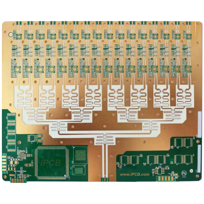
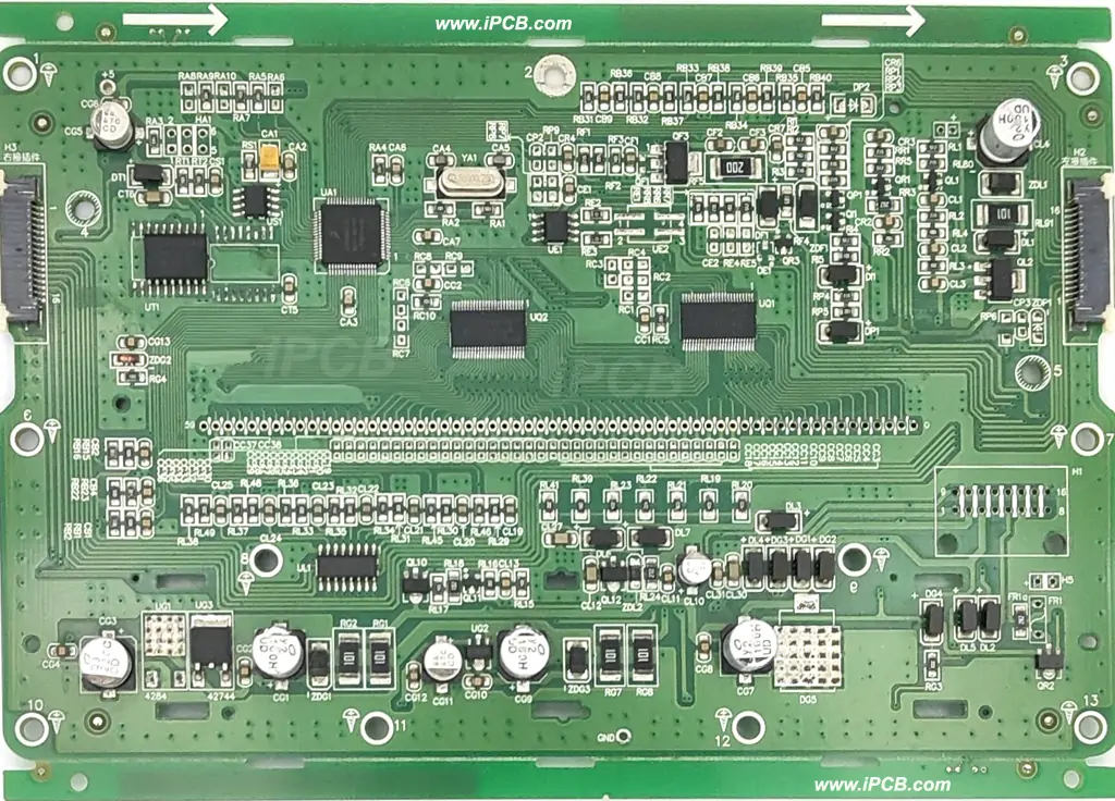
In PCBA, SMT significantly improves production efficiency, reduces costs, and promotes the miniaturization of electronic products by directly mounting electronic components on the PCB surface, compared to traditional DIP.
SMT is an assembly method that attaches surface-mount devices (SMDs) directly to the PCB surface. These components are typically compact and feature flat or leadless pins, making them suitable for high-density circuit layouts. The PCBA process connects components to the PCB through soldering, ensuring stable electrical performance and reliable mechanical connections.
Surface-mount components (SMDs): These include resistors, capacitors, diodes, transistors, and integrated circuits (ICs), designed specifically for mounting.
Solder paste: A mixture of tiny solder particles and flux used to temporarily secure components and create conductive connections.
PCB: A circuit board with conductive paths for connecting mounted components.
Reflow oven: A reflow oven uses precise heat to melt the solder paste, permanently connecting components to the PCB.

pcb
How is SMT used for mounting?
1. Solder Paste Printing
A precision stencil is used to apply solder paste to the component pads on the PCB, ensuring accurate placement and providing adhesion for subsequent component placement.
2. Component Placement
Automated pick-and-place machines utilize vision recognition systems to precisely place SMDs on the solder paste, with high speed and accuracy.
3. Reflow Soldering
The PCB passes through a reflow oven, where the solder paste melts at controlled high temperatures, forming a strong electrical and mechanical connection. After cooling, the solder joints solidify, completing the assembly.
4. Inspection and Testing
After assembly, automated optical inspection (AOI) or X-ray inspection is used to inspect solder joint quality and identify defects such as misalignment or shorts. Functional testing ensures proper function of the board.
5. Cleaning and Post-Processing
The boards are cleaned to remove flux residue and other contaminants. Conformal coating may be applied as needed to protect the boards from environmental influences.
What are the advantages of using SMT technology? Miniaturized Design: SMD components are small, allowing for high-density layouts, making them suitable for compact products such as smartphones and wearables.
Cost-Effectiveness: Automated production reduces labor costs, while smaller PCB sizes reduce material consumption.
Efficient Production: High-speed placement machines and reflow soldering technology support large-scale, rapid production.
Performance Optimization: Short-path design reduces signal interference and improves circuit performance.
Versatility: Supports a variety of component types, adapting to a wide range of applications.

pcba
Challenges of SMD Technology: Component Fragility: SMDs are sensitive to electrostatic discharge (ESD) and improper handling, making them easily damaged.
Thermal Management: Reflow soldering requires precise temperature control to prevent component overheating and damage.
Repair Difficulty: Small components and dense layouts complicate rework and require specialized equipment.
Initial Investment: SMD production lines require high-cost equipment, such as placement machines and reflow ovens.
PCBA SMD technology is a pillar of modern electronics manufacturing. Its efficiency, miniaturization, and versatility have driven the rapid development of the electronics industry. By understanding its processes, advantages, and challenges, companies can better utilize SMD technology to meet market demands. In the future, with the continuous innovation of technology, PCBA technology will play a greater role in the fields of smart devices, green manufacturing and flexible electronics.