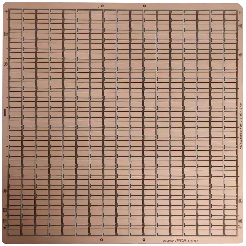
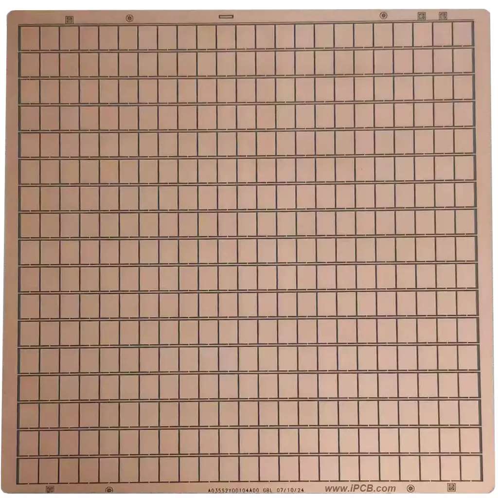
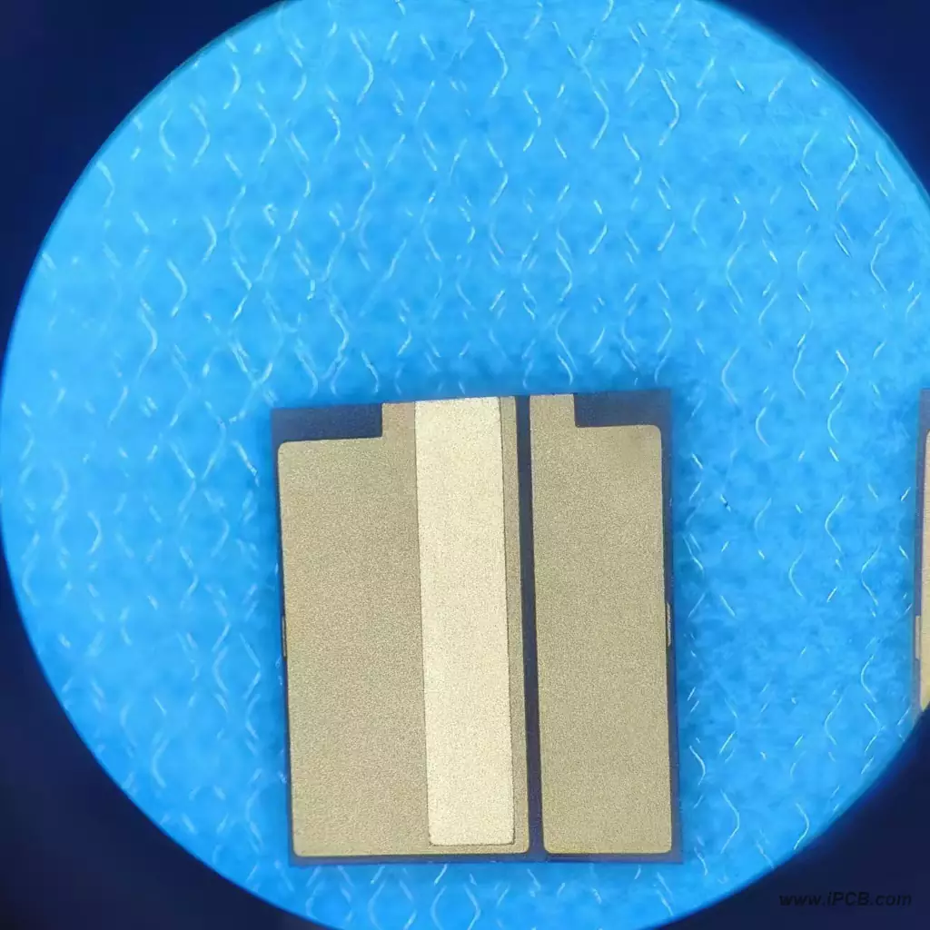
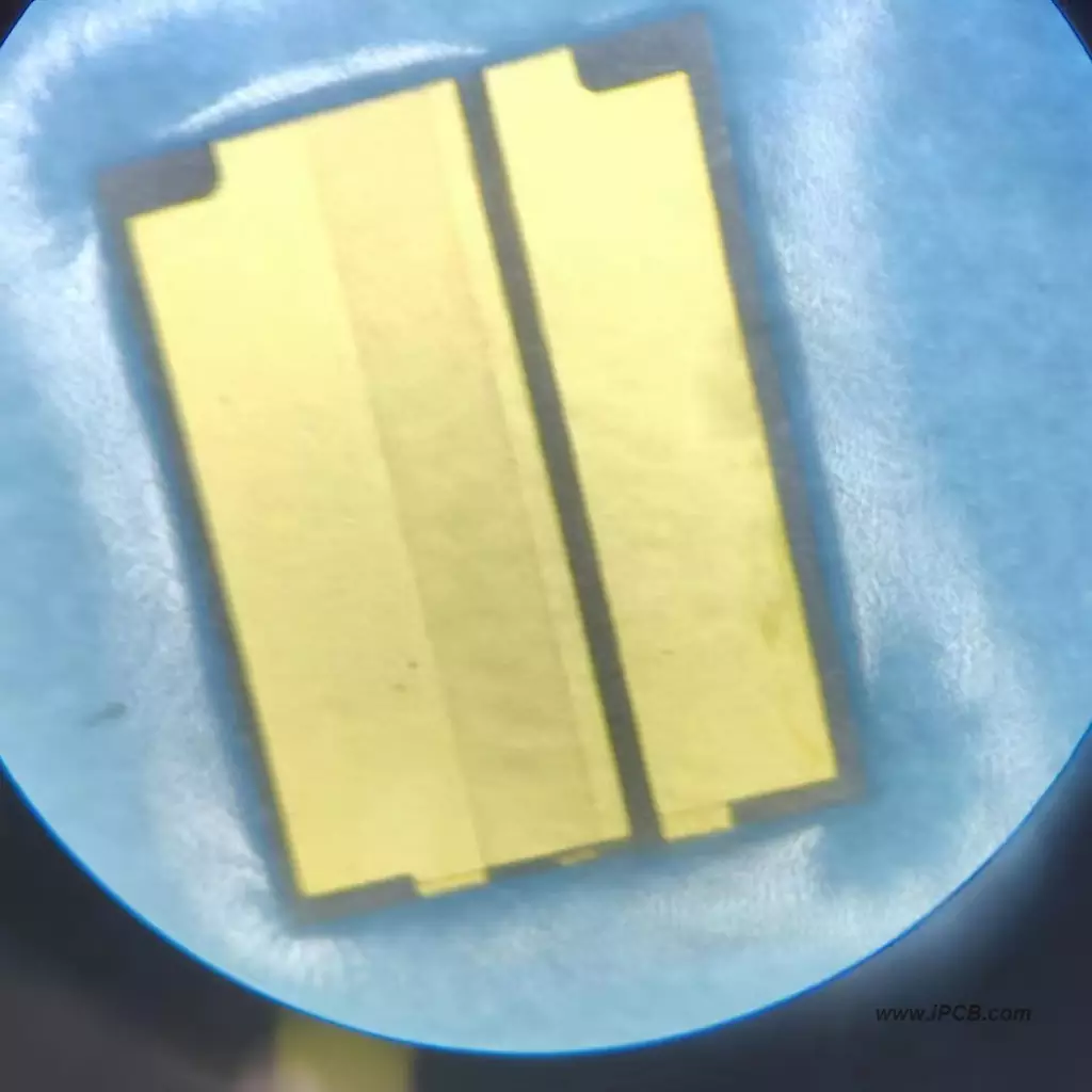
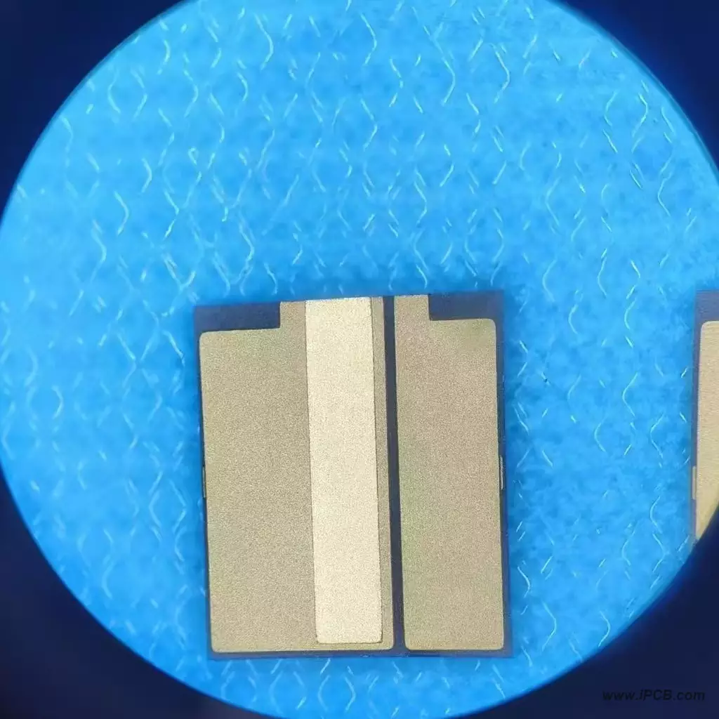
Product Name: AuSn Heat Sink Substrate
Layers: 2
Thickness: 0.25mm
Copper thickness: 18-35um
Composition of solder layer: Au70Sn30, Au75Sn25
Solder layer thickness: 2-10 m ± 20%
Substrate materials: aluminum nitride, aluminum oxide, tungsten copper, molybdenum copper, quartz, silicon
Metalization layer: Ti/Pt/Au, Ti/Ni/Au,Cu/Ni/Au, Cu/Ni/Pd/Au
Customized metalization layer according to customer requirements
Application: High power chip, high-power laser
AuSn heat sink is a substrate with a surface coated with AuSn solder layer, which has been widely used in the optoelectronic industry. The solder thickness in the bonding area of the AuSn thin film heat sink can be accurately controlled, and there is no need to use additional pre-formed solder pads or solder paste, which can be directly soldered.
A heat sink refers to an object whose temperature does not change with the magnitude of the heat energy transferred to it, such as the atmosphere or the earth. Usually, there are several classifications of heat sink:
1. In industry, it refers to a miniature heat sink used to cool electronic chips.
2. In aerospace engineering, it refers to a device that simulates the cold black environment of space by coating the inner surface of liquid nitrogen wall panels with black paint.
3. Currently, in LED lighting packaging, due to the high heat generated when the LED emits light, copper pillars with high thermal conductivity are used to direct the heat outside the packaging. This LED copper pillar is also called a heat sink. LD (laser diode) also generates a lot of heat and needs to be installed on a heat sink to help dissipate heat and stabilize the operating temperature.
Characteristics of AuSn Heat Sink
1. Physical vapor deposition method, with AuSn solder layer thickness ranging from 2μm to 10μm.
2. Alloy film with precise composition.
3. We can provide finished products and AuSn coating processing services.
4. Possess the full process capability of photolithography, coating, and slicing for thin film circuit technology.
5. AuSn alloy has a lower melting point and a moderate brazing temperature, greatly shortening the entire brazing process. The AuSn alloy ceramic circuit board uses AuSn solder, and the brazing temperature is only 20-30 ℃ (about 300-310) higher than its melting point. Because the AuSn alloy is eutectic, the alloy melts faster and solidifies faster. The assembly of components with high stability requirements is generally more suitable for AuSn alloys.
6. Can meet high-strength airtightness requirements at high temperatures of 250-260 ℃.
7. Good wettability, with good wettability and no corrosion of lead-tin solder on the gold plating layer. Because the composition of AuSn alloy is similar to that of the gold plating layer, the immersion degree of very thin coatings through diffusion is very low, and there is no migration phenomenon like silver.
8. Low viscosity - able to fill large gaps and maintain stability without fluidity.
9. Good thermal conductivity due to its solder material having high corrosion resistance, high creep resistance, and good thermal and electrical conductivity, with a thermal conductivity coefficient of 57 W/mK.
10. Lead-free and environmentally friendly.
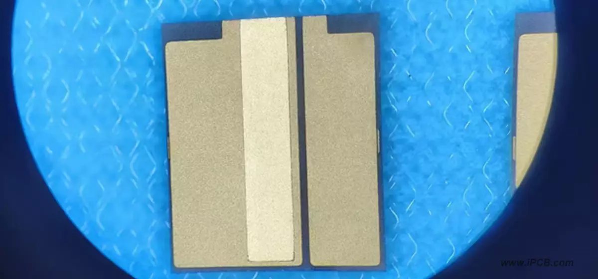
AuSn Heat Sink
Disadvantages of AuSn Heat Sink
1. Expensive price, brittle performance, low elongation, and difficult to process.
2. Due to its high melting point, it cannot be welded simultaneously with low melting point solder.
3. It can only be applied in situations where the chip can withstand short-term temperatures above 300℃.
4. Excessive gold plating, thin solder pads, and prolonged soldering time can increase the diffusion of gold into the solder, leading to an increase in melting point.
Specification parameters of AuSn heat sink
Composition of solder layer: Au70Sn30, Au75Sn25.
Solder layer thickness: 2-10 μ m ± 20%.
Substrate materials: aluminum nitride, aluminum oxide, tungsten copper, molybdenum copper, quartz, silicon, etc.
Metalization layer: Ti/Pt/Au, Ti/Ni/Au, Cu/Ni/Au, Cu/Ni/Pd/Au, etc. The metalization layer can be customized according to customer requirements.
Application of AuSn Heat Sink
1. Laser diode: AuSn alloy has important applications in laser packaging in optoelectronics. In the next five years, AuSn alloy will be an important packaging material for the promotion of optical communication and photon computers.
2. Application in high-power LEDs: Improving the heat dissipation capacity of high-power LEDs through chip packaging is the core issue that LED device packaging and application design need to address the ultrasonic image of the interface between germanium wafer and gallium arsenide wafer bonded by AuSn.
3. In the application of IC and power semiconductor devices, AuSn20 alloy solder is the only solder with a melting point between 280~360 ℃ that can replace high melting point lead-based alloys. AuGe and AuSi are mainly used for the connection between chips and circuit substrates, while AuSn20 solder can be widely used for various high-reliability circuit airtight packaging in addition to the connection between chips and circuit substrates.
4. Electroplating AuSn alloy pads are used in thin-film integrated circuits. The advantages of AuSn heat sink technology for ceramic substrates are obvious. The Au80/Sn20 solder formed by the AuSn alloy electroplating method has broad application prospects in fields such as microelectronics, optoelectronics, semiconductor luminescence, and MEMS, and has been put into production and application.
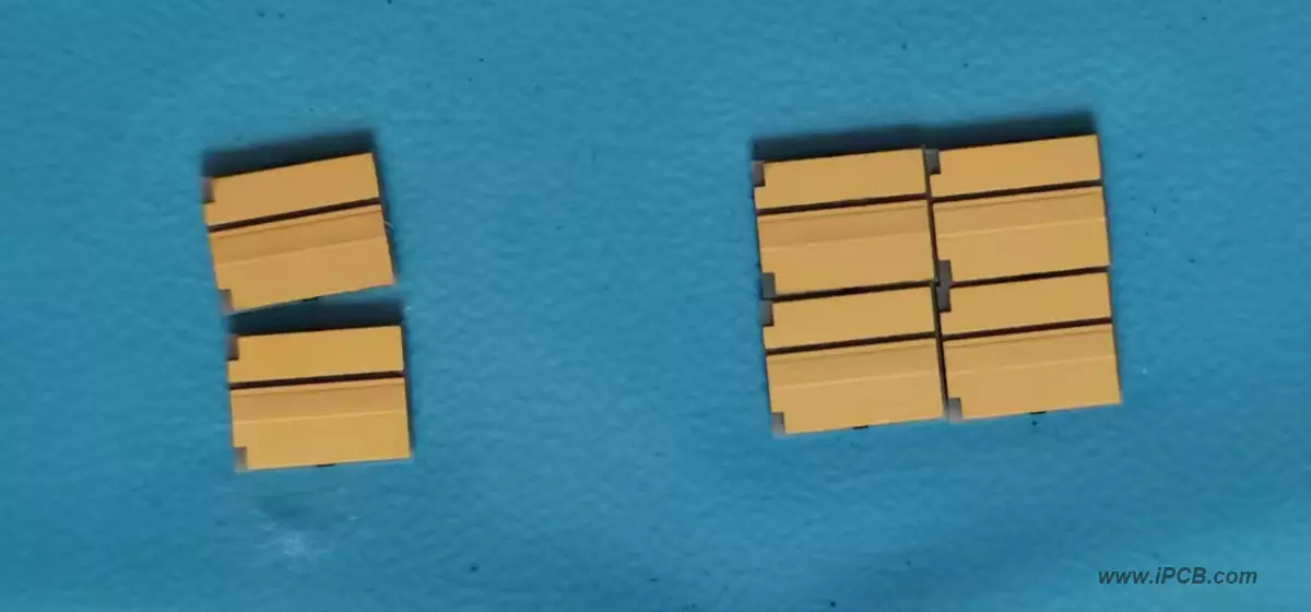
AuSn Heat Sink
With the upgrading of demand, the trend of miniaturization of laser chips is obvious. However, small chips have low heat dissipation, small temperature difference between working and non-working heat sink, and low thermal matching requirements. Aluminum nitride material can be used as the substrate to connect with the chip. In the field of electronic packaging, heat sink mainly refers to miniature heat sinks, which are used to cool electronic chips and are one of the core components. Traditional heat sink products have significant room for improvement in assembly efficiency, reliability, performance, and other aspects. Ceramic heat sink can meet the bonding needs of high-power semiconductor laser chips and have broad application prospects in fields such as optical communication, high-power LED packaging, semiconductor lasers, and fiber laser pump source manufacturing.
Product Name: AuSn Heat Sink Substrate
Layers: 2
Thickness: 0.25mm
Copper thickness: 18-35um
Composition of solder layer: Au70Sn30, Au75Sn25
Solder layer thickness: 2-10 m ± 20%
Substrate materials: aluminum nitride, aluminum oxide, tungsten copper, molybdenum copper, quartz, silicon
Metalization layer: Ti/Pt/Au, Ti/Ni/Au,Cu/Ni/Au, Cu/Ni/Pd/Au
Customized metalization layer according to customer requirements
Application: High power chip, high-power laser
iPCB Circuit provides support for PCB design, PCB technology, and PCBA assembly. You can request technical consultation or quotation for PCB and PCBA here, please contact email: sales@ipcb.com
We will respond very quickly.