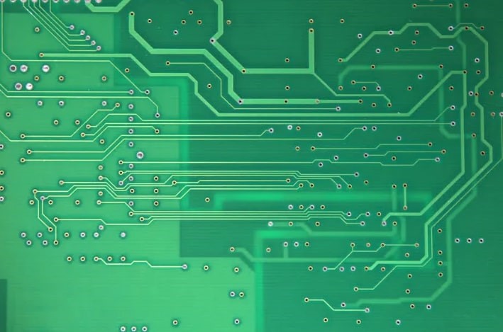
A bare PCB, also known as a blank PCB, is a printed circuit board that does not have any electronic components installed. These boards typically have a substrate, copper foil alignment, soldermask and screen printing. However, in the absence of components, a bare PCB only provides electrical access and does not have the functionality required for the design. It needs to undergo subsequent processes, such as soldering and assembly, to become a complete circuit board for its intended use.
What is a bare board?
In PCB terminology, the term "bare board" refers to the state of a PCB before electronic components or vias are installed. A bare board consists of the PCB's substrate, metallic coating, conductive paths and patterns. Some industry experts refer to bare boards as PCBs and assembled boards as PCBAs.
Basic Components of a Bare Board
Every complex PCB originates from a basic bare board. Despite its unassuming name, this basic component plays a vital role by housing the essential components that support complex electronic devices. The following are the basic components that make up the essence of a bare board:
Substrate: The foundation that provides mechanical support and electrical insulation. Made from materials such as FR4 (fiberglass and epoxy laminate) to balance strength and heat resistance. Special applications may use polyimide (flexible and heat resistant) or ceramic composites (excellent heat conductors).
Copper Wire: Highway that forms the conductive path for electrical signals. Etched into the substrate for precise connections. Width and thickness determine current capacity and signal integrity. Technological advances have enabled finer traces for miniaturization and improved performance.
Vias: Bridges that connect different layers in a multi-layer PCB to achieve complex interconnections. Types of vias include:
Through-hole vias: Drill through the entire board for a strong connection.
Blind Vias: Connects the outer layer to the inner layer without penetrating the board.
Buried vias: exist entirely within the inner layer. Materials such as copper plating ensure reliable connections across layers, resulting in compact and fully functional PCBs. advances in through-hole technology (laser drilling, plating methods) have enhanced design flexibility and performance.

A Bare PCB
What are the advantages of a bare PCB?
Firstly, it allows designers to test circuits and try out new ideas at a very low cost, and then, once the circuit is correct, transfer it to a finished board for soldering and assembly. Secondly, bare PCBs can be used to make your own when a public PCB cannot meet your design needs, which is why DIY electronics enthusiasts widely use bare PCBs.
Of course, there are some disadvantages of using bare PCBs. First of all, even good designers are difficult to ensure the overall quality and stability of the bare board design, so detailed testing and inspection is required. Secondly, for small production runs and personal use, using bare PCBs may be more cost effective, but for mass production, the cost of making bare boards becomes higher.
In printed circuit board manufacturing, bare PCB testing may be encountered (mainly used to monitor PCBs for possible defects in the production process, such as open circuits, short circuits, misalignments, etc., so as to ensure the smoothness of subsequent assembly and use). The following are several commonly used PCB bare board test program:
1, AOI test (automatic optical inspection)
AOI test is a method of using high-precision cameras and image processing technology to detect defects on the bare PCB. It identifies possible defects by capturing the PCB image and comparing it with a preset standard image.
AOI test has the advantages of fast speed, high accuracy and good repeatability, and is suitable for rapid inspection of large-scale production lines;
2、Flying needle test
Flying probe test is a contact test method to measure the connectivity between circuits by contacting the test points on the PCB bare board with tiny probes. It can detect open circuits, short circuits and other electrical performance issues, for complex circuits and tiny spacing of the test point has a high degree of accuracy.
Although the flying probe test is relatively slow, but the test accuracy is high, suitable for high-precision requirements of PCB products;
3、Fixture test
Fixture test is a specially designed test fixtures on the bare PCB test method. Fixture on the pins and PCB test points correspond to each other, by connecting the test instrument, you can detect the circuit's various performance indicators.
Fixture testing has a high degree of testing accuracy and reliability, suitable for mass production and customized testing needs;
4, manual visual inspection
Although manual visual inspection is simple and intuitive, through experienced workers with the naked eye to observe the PCB bare board, to identify possible defects.
Although the speed and accuracy of manual visual inspection is affected by the experience and fatigue level of workers, manual visual inspection still has some practical value in some specific cases, such as small batch production or special customized products.
Benefits of Bare PCB Testing
Cost Savings: Extensive testing in the early design phase can help you save on the costs associated with defective assembled PCBs.
Streamline Production: By identifying problems during the prototyping phase, you can save time during the later production phase.
Problem Solving: Bare board testing will help you identify potential problems early in production while narrowing down the root cause of each problem.
In short, bare PCB as an important part of electronic components, in accelerating electronic design, shorten the development cycle has a very important role. PCB circuit board bare board of continuous development and innovation, will provide a solid support for the progress of electronic technology, to bring us a more intelligent, convenient and efficient electronic life!