A Trustworthy PCB and Electronic Manufacturing Enterprise! Contact Us


In the past 30 years,the electronics industry chain has received unprecedented development opportunities.Various electronic products have developed rapidly following the market.For manufacturers in the electronics manufacturing field,it has become crucial to improve processing levels and capture market share.
There are many types of chip packaging technologies,such as COB,QFN,BGA,PLCC,etc.As for which packaging pipeline is used,it depends on the structure of the chip.
As far as SMT patch processing is concerned,BGA welding and LGA welding can be regarded as a relatively difficult process.In the past few years,during the production of XRAY testing equipment,we often encountered the need to use XRAY to detect BGA welding,SMT patch and other processes.The qualification rate of the final product.
What is the difference between BGA packaging and LGA packaging?
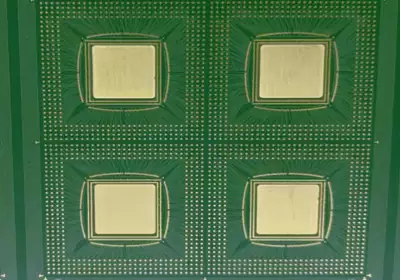
The full name of BGA is BALL GRID ARRAY, which means ball grid array package.
The BGA Package uses spherical solder joints to connect the chip and the motherboard.These spherical solder joints are located on the bottom of the chip.When installing a BGA packaged chip,it is usually necessary to use a heat gun or coolant to heat or cool the chip so that the ball solder joints on the bottom can be bonded to the pads on the motherboard.

BGA Package
The full name of LGA is LAND GRID ARRAY, which means plane grid array package. The LGA package is basically the reverse of the BGA package.It places the solder joints on the bottom of the motherboard.LGA packaged chips have many small binding posts that easily plug into holes in the motherboard. After creating the circuit connections, add a heat sink on top of the wafer.

LGA Package
BGA package and LGA package are very different from every angle.
1. The BGA package is relatively small and has no pins for soldering.
2. The BGA package uses pinless welding. The pins cannot be seen from the outside. It is a disposable packaging pipeline. Once welded, you need to use professional tools if it needs to be disassembled. The pins for the LGA package are all welded on the motherboard. It can be seen and can be replaced individually.
3. The BGA package is smaller than the LGA package and has relatively weak thermal conductivity.
4. The larger the size, the higher the power consumption. The BGA package is smaller than the LGA package, so the power consumption is also smaller. This is also the reason why BGA chips are getting smaller and smaller. The smaller they carry, the less power consumption they carry, and they are more competitive in all aspects, such as longer standby time and higher cost performance.