A Trustworthy PCB and Electronic Manufacturing Enterprise! Contact Us


BGA package, also known as ball grid array package, is an array of solder balls made on the bottom of the package substrate as the I/O end of the circuit to interconnect with the printed circuit board (PCB). The device packaged using this technology is a surface mount device.
BGA package classification
1. PBGA (Plastic BGA) substrate: generally a multilayer board composed of 2-4 layers of organic materials. Among Intel series CPUs, Pentium II, III, and IV processors all use this packaging form. In the past two years, another form has emerged: binding the IC directly to the board. Its price is much cheaper than the regular price. It is generally used in games and other fields that do not have strict quality requirements.
2. CBGA (CeramicBGA) substrate: that is, a ceramic substrate. The electrical connection between the chip and the substrate usually uses a flip-chip (FC) installation method. Among Intel series CPUs, Pentium I, II, and Pentium Pro processors have all adopted this packaging form.
3. FCBGA (FilpChipBGA) substrate: rigid multi-layer substrate.
4. TBGA (TapeBGA) substrate: The substrate is a strip-shaped soft 1-2 layer printed circuit board.
5. CDPBGA (Carity Down PBGA) substrate: refers to the square depressed chip area (also called the cavity area) in the center of the package

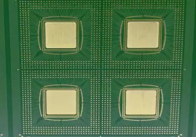
BGA Pakage
There are currently many IC packaging styles, each with its own merits. For example, the more mainstream packaging pipelines include BGA packaging, SOP packaging, QFN packaging, PLCC packaging, SSOP packaging, QFP packaging, etc. So today we share the advantages and disadvantages of BGA packaging.
Advantages of BGA packaging
1. The BGA is small in size but has a large memory capacity. For the same memory IC with the same capacity, the BGA volume is only one third of the SOP package.
2. QFP and SOP package pins are distributed around the body. When there are many pins and the spacing is reduced to a certain extent, the pins are easy to deform and bend. However, the BGA solder balls are at the bottom of the package, and the spacing increases instead, which greatly improves the yield rate.
3. The electrical performance is good, the BGA pins are very short, solder balls are used instead of leads, and the signal paths are short. The lead inductance and capacitance are reduced and the electrical performance is enhanced.
4. Good heat dissipation. The spherical contact array and the contact surface of the substrate form a gap, which is beneficial to the heat dissipation of the body.
5. The BGA body and the PCB board have good coplanarity, which can effectively ensure the welding quality.
Disadvantages of BGA packaging
1. Quality inspection and maintenance after BGA welding are difficult. X-Ray perspective inspection must be used to ensure the electrical performance of the welded connection. The inspection quality cannot be judged by the naked eye and AOI.
2. The BGA pins are at the bottom of the body, which can easily cause welding shadow effects. Therefore, the welding temperature curve is required to be high. The actual welding temperature must be monitored in real time.
3. If individual solder joints of the BGA pins are poorly welded, the entire BGA must be removed and re-balled, and then the second patch welding must be performed. Affects pass-through rate and electrical performance.
4. The BGA package is very reliable. Compared with the 20mil pitch QFP, the BGA has no pins that can be bent or broken. The welding is firm. Generally, if you want to remove the BGA package, you must use a BGA rework station to remove it at high temperature.

BGA package substrate
There are many types of BGA packages, and their shape structures are square or rectangular. According to the arrangement of its solder ball channels, it can be divided into peripheral type, staggered type and full array type BGA. According to its different substrates, it is mainly divided into three categories: PBGA (PlasticballZddarray plastic solder ball array), CBGA (ceramicballSddarray ceramic solder ball array) ), TBGA (tape ball grid array carrier tape type solder ball array).
PBGA (Plastic Ball Array) Package
PBGA package, which uses BT resin/glass laminate as the substrate, plastic (epoxy molding compound) as the sealing material, and the solder ball is eutectic solder 63Sn37Pb or quasi-eutectic solder 62Sn36Pb2Ag (some manufacturers have used lead-free solder ), the connection between the solder ball and the package body does not require the use of additional solder. Some PBGA packages have a cavity structure, which is divided into two types: cavity upward and cavity downward. This kind of PBGA with a cavity is called thermally enhanced BGA, or EBGA for short, in order to enhance its heat dissipation performance. Some also call it CPBGA (cavity plastic ball array).
The advantages of PBGA packaging are as follows:
1. Good thermal matching with PCB board (printed circuit board - usually FR-4 board). The thermal expansion coefficient (CTE) of the BT resin/glass laminate in the PBGA structure is about 14ppm/℃, and that of the PCB board is about 17ppm/cC. The CTE of the two materials is relatively close, so the thermal matching is good.
2. During the reflow soldering process, the self-alignment effect of the solder ball, that is, the surface tension of the molten solder ball, can be used to achieve the alignment requirements of the solder ball and the pad.
3. Low cost.
4. Good electrical performance.
The disadvantage of PBGA packaging is that it is sensitive to moisture and is not suitable for packaging devices with air tightness and high reliability requirements.
CBGA (ceramic ball array) package
Among the BGA packaging series, CBGA has the longest history. Its substrate is a multi-layer ceramic, and the metal cover is welded to the substrate with sealing solder to protect the chip, leads and pads. The solder ball material is high-temperature eutectic solder 10Sn90Pb, and the connection between the solder ball and the package requires low-temperature eutectic solder 63Sn37Pb. Standard solder ball pitches are 1.5mm, 1.27mm, and 1.0mm.
The advantages of CBGA (Ceramic Ball Array) packaging are as follows:
1. It has good air tightness and high moisture resistance, so the long-term reliability of the packaged components is high.
2. Compared with PBGA devices, the electrical insulation properties are better.
3. Compared with PBGA devices, the packaging density is higher.
4. The heat dissipation performance is better than that of PBGA structure.
The disadvantages of CBGA packaging are:
1. Due to the large difference in thermal expansion coefficient (CTE) between the ceramic substrate and the PCB board (the CTE of the A1203 ceramic substrate is about 7ppm/cC and the CTE of the PCB board is about 17ppm/pen), the thermal matching is poor and solder joint fatigue is Its main failure modes.
2. Compared with PBGA devices, the packaging cost is high.
3. The solder ball alignment at the edge of the package becomes more difficult.
CCGA (ceramiccolumnSddarray) ceramic column grid array
CCGA is an improved version of CBGA. The difference between the two is that CCGA uses solder pillars with a diameter of 0.5mm and a height of 1.25mm~2.2mm to replace the 0.87mm diameter solder balls in CBGA to improve the fatigue resistance of its solder joints. This columnar structure can better alleviate the shear stress between the ceramic carrier and the PCB board caused by thermal mismatch.
TBGA (Tape Ball Array)
TBGA is a cavity structure. There are two types of interconnection pipes between the chip and the substrate of TBGA package: flip-chip bonding and wire bonding. Flip-chip soldering bonding structure; the chip is flip-chip bonded on a multi-layer wiring flexible carrier tape; the peripheral array solder balls used as the I/O end of the circuit are installed under the flexible carrier tape; its thick sealing cover is also a heat sink ( heat sink), and also plays a role in reinforcing the package, so that the solder balls under the flexible substrate have better coplanarity.
The advantages of TBGA are as follows:
1. The thermal matching performance of the flexible carrier tape of the package and the PCB board is relatively poor.
2. During the reflow soldering process, the self-alignment effect of the solder ball can be used to achieve the alignment requirements of the solder ball and the pad by printing the surface tension of the solder ball.
3. It is the most economical BGA package.
4. The heat dissipation performance is better than that of PBGA structure.
The disadvantages of TBGA are as follows:
1. Sensitive to moisture.
2. Multi-level combinations of different materials have an adverse impact on reliability.

PCB substrate with BGA package