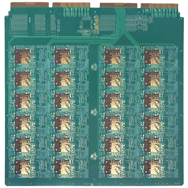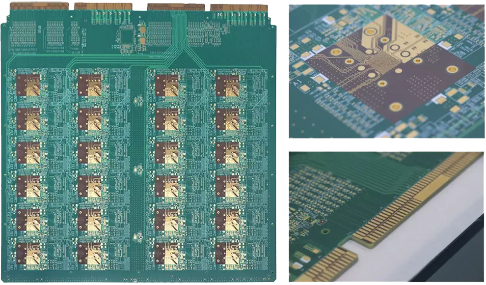
Product name: Burn In Board (BIB)
Material: High TG FR4
Layer: 16L
Finished size: 20"*22"
Surface treatment: Immersion Gold
Flatness: 0.3%
Product Application: Chip Burn in testing
Burn In Board (BIB) testing is a screening method used to eliminate defective components in fully processed microelectronic components using accelerated aging. This screening is obtained by applying pressure operating conditions. In addition to the increased voltage and temperature, dynamic aging also applies external signals to the parallel input pins of all chips, solving the potential problem that not all nodes are under pressure. This technology requires complete product functionality under aging conditions, but can improve aging efficiency and easily achieve parallel stress on many parts.
Burn in board testing is conducted to accelerate chip aging at high temperatures in order to understand the potential failure analysis of the product, resulting in premature occurrence of faults. For example, a problem that could have occurred in 3 years would appear in 10 days at high temperatures, mainly because the electron migration rate increases and the atomic barrier effect becomes more pronounced at high temperatures. Some places are also called aging tests directly, and there are actually overlapping areas between the two.
Burn in board precautions
1. Chip operates at full load
Load board must be designed first to provide necessary signal inputs. The most common working state configuration. The various parts of the chip need to work at full speed. If it is a digital chip, it may involve the requirement of inputting some test vectors.
2. Comprehensive monitoring
Continuous monitoring is required 24 hours a day during the experiment, and it is best to design some automatic recording software. The board may involve some necessary data acquisition interfaces, such as chip current monitoring and key voltage monitoring for RFID.
3. High temperature work
High temperature design is necessary in order to accelerate aging and identify fault points in advance. As for how much temperature is appropriate, the requirements of each chip and even different companies vary. The time of the first failure is crucial for recording the experiment, but it may not be appropriate to have someone record it. This is one of the reasons. Secondly, it is best to leave the experimental site earlier for the load board after the first failure occurs, in order to consider subsequent failure analysis. If it is too late or too slow, some chips may have a series of chain reactions, which is not conducive to subsequent failure analysis.
4. Analysis is the result
The purpose of conducting Burn in testing is for analysis, so it is important to provide as many experimental samples as possible. The usual first step in analysis is to take photos and find the fault point. Generally, testing engineers do not know the ultimate cause of the fault, so after taking photos, it is necessary to submit them to the designer for analysis. The two must interact frequently to finally find the fault point. For example, when inspecting the burnt debris of a chip, taking photos may not immediately find the ignition point. With the assistance of the designer, it may be necessary to enlarge certain areas for analysis.
5. Improvement is the goal
With the analysis results, the fault point has been identified, with the aim of improving product yield or discovering fatal issues that require redesign. Or propose measures for product screening schemes.
A good burn in test report needs to report on the testing environment, testing methods, testing result records, analysis reports, and improvement measures in order to be perfect.
The challenges faced by BIB burn in testing include high number of parallel tests, low testing speed, mainly BIST (logic built-in self-test), and a lack of high-temperature and high-speed aging testing equipment.

Burn In Board (BIB)
The advanced type of aging is TDBI (test during burn in aging). TDBI applies full functional testing mode and full response monitoring to each individual chip. The advantage is that accurate fault time and characteristics, as well as equipment or contact issues, can be determined. Therefore, aging leakage can be minimized to the greatest extent possible, and chips that have not been exposed to aging voltage can be recovered. The individual monitoring of each chip limits the number of components that can apply pressure on a Burn In Board (BIB), and the required equipment makes this type of aging typically very expensive.
Product name: Burn In Board (BIB)
Material: High TG FR4
Layer: 16L
Finished size: 20"*22"
Surface treatment: Immersion Gold
Flatness: 0.3%
Product Application: Chip Burn in testing
iPCB Circuit provides support for PCB design, PCB technology, and PCBA assembly. You can request technical consultation or quotation for PCB and PCBA here, please contact email: sales@ipcb.com
We will respond very quickly.