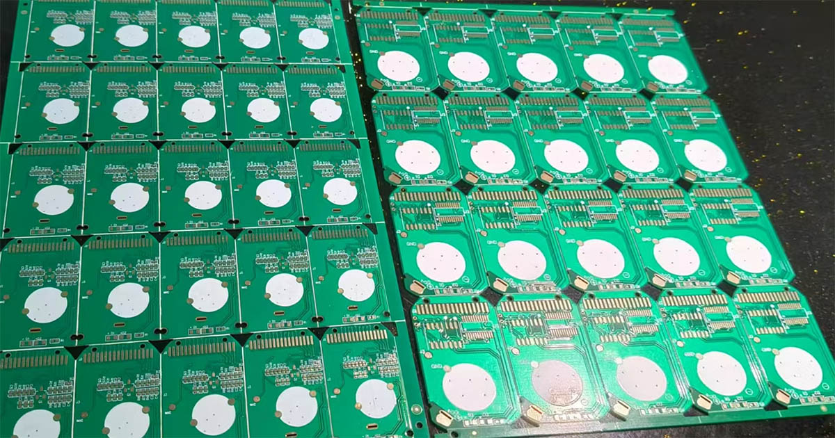
PCB bare boards will experience PCB warpage during PCBA assembly, affecting their yield. In addition, excessive PCB warpage can also cause the quality of paste printing to be affected. During the reflow soldering process, PCB warpage can also affect the formation of solder joints. Before we find solutions that help control PCB warpage, let's quickly understand what PCB warpage is all about?
What is PCB warpage?
Usually all parts of the PCB should be in contact with the surface. However, sometimes this does not happen due to various stresses. We encounter situations where some parts of the PCB board bend upward and some bend downward, resulting in positive and negative curvatures. Sometimes, the bend may be along the axis or diagonal of the board. The PCB sometimes also produces distortion. All of these are examples of PCB warpage.
Causes of PCB Warpage
1. Internal stress on the copper film causes PCB warpage. Even at room temperature, it can be done without any heat treatment.
2. During processes involving temperature changes, such as reflow soldering, PCB warping occurs due to the different coefficients of thermal expansion between the copper layer and the substrate.
3. When individually etched copper spacers are stacked together, the difference in copper density on each layer causes different stresses on each layer, which causes PCB warping.
4. PCBs are usually placed in panels to improve PCBA assembly efficiency. Panels use rails and legs in turn. After PCBA assembly, the legs are removed and the PCBs are separated by removing the panel. The difference in copper density between the PCB board area and the leg area further causes PCB warping.

PCB Warpage
Problems caused by PCB warping of PCBA assembly
In the case of a PCB with PCB warping, some parts of the PCB will be closer to the die, while some parts will be farther away from the die. This, in turn, causes a lower height of solder paste deposits on the closer parts of the PCB. The deposit height is larger on parts with larger gaps. With this uneven solder paste deposition, many problems can be seen. These include:
1. Stretched joints
2. Open joints
3. Solder bridges
4. Pad joints
When the temperature rises, such as during reflow soldering, its PCB warpage increases. In turn, it affects soldering under close-pitch ICs.
Methods to prevent PCBA assembly and PCB warpage
The IPC-A-610E standard specifies the maximum PCB warpage of input PCBs at room temperature. According to IPC-TM-650, the maximum bending and twisting of PCBs in SMT shall not exceed 0.75%.
To control PCB warpage in PCBA assembly, iPCB recommends the following steps:
1. Copper balancing is required during PCB design. During the design phase, attention must be paid to balancing the copper of all layers. This helps to minimize the mismatch in thermal expansion coefficient at room temperature and when the temperature rises.
2. Balance the substrate across PCB layers. In multi-layer PCBs, attention must be paid to using substrates with different CTEs. It is recommended to use substrates of the same thickness and material on the top and bottom layers.
3. Balance the copper density. During the panelization process, the difference in copper density in the panel rail and leg areas needs to be minimized.
4. Pallet design, it is recommended to minimize the temperature difference between the PCB and the pallet. In addition, the gap between the edge of the PCB and the edge of the pallet needs to be kept to a minimum. It is also prudent to use low spring forces to hold down the perimeter and corners of the PCB. It is also recommended to provide adequate support for the pallet so that the PCB does not sag at high temperatures.
5. Pretreatment, baking the PCB to above Tg works well. This helps soften the laminate and can also relieve stress in different layers. As a result, pcb warpage is minimized.