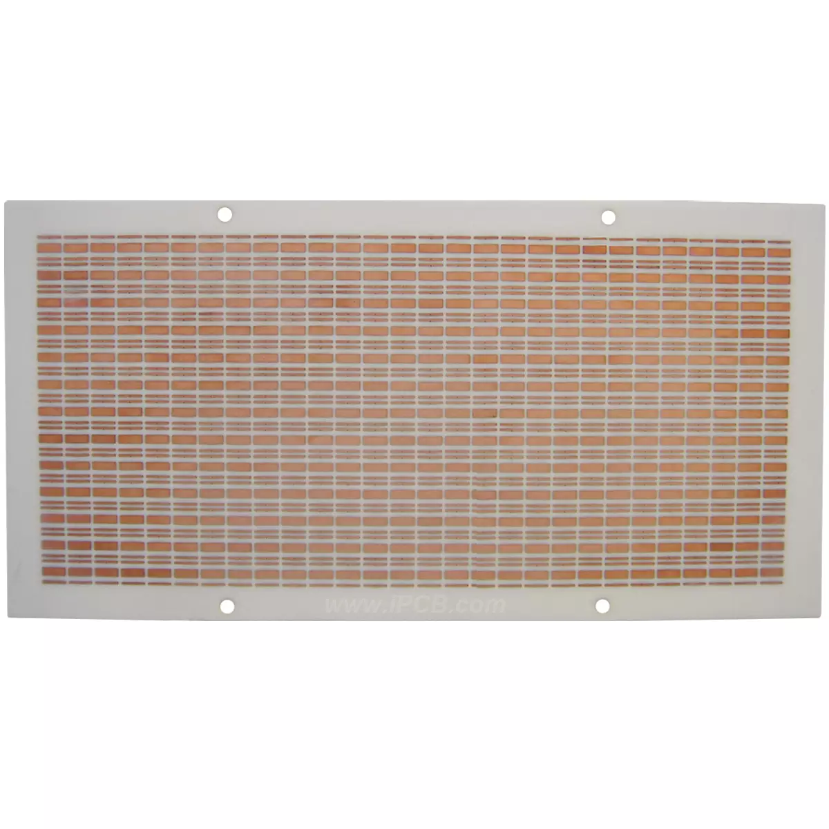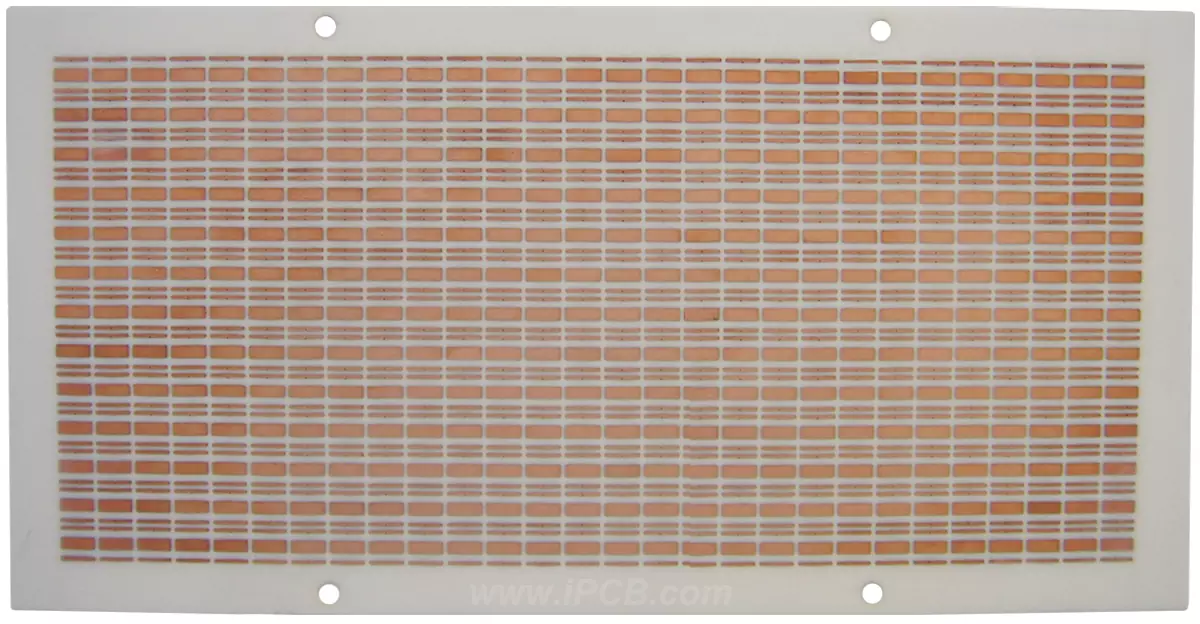
Substrate type: 96% alumina ceramic
Substrate thickness: 0.3-2.0mm
Conductive layer: copper, nickel, gold
Metal layer thickness: 65 μ m
Surface treatment: Nickel gold
Metal : double-sided
Conductive hole: 0.2mm conductive hole
Line width: 0.05mm
Application: High power LED bead
Ceramic circuit board have excellent heat dissipation coefficients, and high integration of circuit boards has become an inevitable trend. Highly integrated packaging modules require a good heat dissipation and load-bearing system. However, the disadvantage of traditional circuit board FR-4 and CEM-3 in terms of thermal conductivity (TC) has become a bottleneck restricting the development of electronic manufacturing. In recent years, the development of the LED industry has also put forward higher requirements for the thermal conductivity (TC) of the circuit board it carries. In the field of high-power LED lighting, metal circuit boards and ceramic circuit boards with good heat dissipation performance are often used. The thermal conductivity of high thermal conductivity aluminum circuit board is generally 1-4W/M.K, while the thermal conductivity of ceramic circuit board can reach around 220W/M.K depending on their manufacturing methods and material formulations.
Advantages of Ceramic Circuit Board
Unlike traditional FR-4, ceramic circuit board have excellent high-frequency and electrical properties, as well as high thermal conductivity, chemical stability, and thermal stability that organic substrates do not possess. They are ideal packaging materials for the new generation of large-scale integrated circuits and power electronic modules.
1. Higher thermal conductivity
2. More matching coefficient of thermal expansion
3. A more robust and lower resistance metal film layer
4. Ceramic circuit boards have good solderability and high operating temperatures
5. Good insulation performance
6. Low high-frequency loss
7. Can be assembled with high density
8. Does not contain organic components, is resistant to cosmic rays, has high reliability in aerospace, and has a long service life
9. The copper layer does not contain an oxide layer and can be used for a long time in a reducing atmosphere

Ceramic Circuit Board
Common processes for ceramic circuit board
The manufacturing methods of traditional ceramic circuit boards can be divided into four categories: HTCC, LTCC, DBC, DPC.
1. The HTCC (high-temperature co firing) manufacturing method requires a temperature of over 1300 ° C, but the manufacturing cost is quite expensive due to the influence of electrode selection.
2. The manufacturing of LTCC (Low Temperature Co firing) requires a calcination process of about 850 ° C, but the precision of the manufactured circuit is poor, and the thermal conductivity of the finished product is low.
3. The manufacturing method of DBC requires the formation of an alloy between copper foil and ceramics, and strict control of the calcination temperature within the temperature range of 1065-1085 ° C. Due to the manufacturing method of DBC ceramic circuit board requiring copper foil thickness, which generally cannot be less than 150-300 microns, the wire width to depth ratio of such ceramic circuit board is limited.
4. The manufacturing methods of DPC include vacuum coating, wet coating, exposure development, etching and other process steps, so the price of its products is relatively high. In addition, in terms of shape processing, DPC ceramic circuit board require laser cutting, which traditional drilling and milling machines and punching machines cannot accurately process. Therefore, the bonding force and line width of DPC ceramic circuit board is also more precise.
Substrate type: 96% alumina ceramic
Substrate thickness: 0.3-2.0mm
Conductive layer: copper, nickel, gold
Metal layer thickness: 65 μ m
Surface treatment: Nickel gold
Metal : double-sided
Conductive hole: 0.2mm conductive hole
Line width: 0.05mm
Application: High power LED bead
iPCB Circuit provides support for PCB design, PCB technology, and PCBA assembly. You can request technical consultation or quotation for PCB and PCBA here, please contact email: sales@ipcb.com
We will respond very quickly.