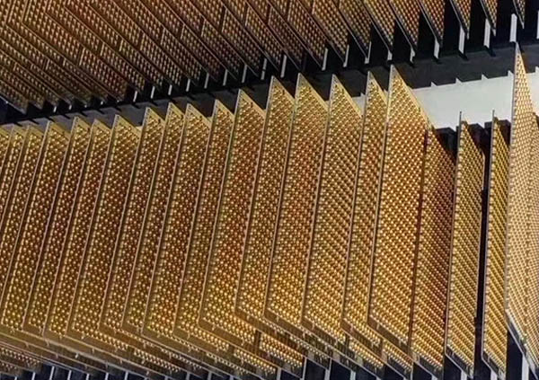
Laser Processing of ceramic circuit boards principle
Laser processing is the use of light energy after focusing the lens to achieve a high energy density, relying on the photo thermal effect to carry out the treatment. Laser processing requires no tools, is fast, has little surface deformation, and can process a variety of materials. Laser beams are used to treat a variety of materials, such as punching, cutting, slicing, welding, and heat treatment. Some substances with sub-stable energy levels will absorb light energy when stimulated by external photons, making the number of high-energy atoms larger than the number of low-energy atoms - particle number reversal. If there is a beam of light, the energy of the photon is equal to the corresponding difference between these two energies, and then excitation radiation is produced, outputting a large amount of light energy.
Characteristics of laser processing ceramic circuit boards
1.Laser power density is high, the workpiece absorbs the laser and the temperature rises rapidly, melting or evaporating. Even high melting point, hardness and brittle materials such as ceramics and diamond can be processed by laser. can also be processed by laser.
2.No contact between laser head and workpiece, no wear and tear of processing tools.
3.The workpiece is not subject to stress and is not easily contaminated.
4.It is possible to process the moving workpiece or material which is sealed in the glass case.
5.The dispersion angle of the laser beam can be less than 1m arc, the spot diameter can be less than micron level, the action time can be as short as nanoseconds and picoseconds. At the same time, the continuous output power of high-power lasers can reach the level of kilowatts to ten kilowatts. In this way, the laser is not only suitable for fine processing, but also for large-scale material processing.
6.The laser beam is easy to control, easy to combine with precision machinery, precision measurement technology and electronic computers to achieve a high degree of automation of processing, to achieve higher processing accuracy.
7.The robot can be used in harsh environments or other people are difficult to access the place for laser processing.

ceramic circuits board
Advantages of laser processing of ceramic pcb
Laser processing is a non-contact process in which the energy of the high-energy laser beam and its speed of travel can be adjusted to achieve a wide range of processing objectives. It is possible to process a wide range of metallic and non-metallic materials, especially those with high hardness, brittleness and melting point. Flexibility in laser processing is mainly used for cutting, surface treatment, welding, marking and punching. Laser surface treatment includes laser phase hardening, laser melting, laser surface alloying and laser surface condensation.
1.The use of laser processing of ceramic circuit boards has high production efficiency, reliable quality and high economic benefits.
2.Workpieces in closed containers can be processed through transparent media, and robots can be used for laser processing in harsh environments or other inaccessible places.
3.Laser processing of ceramic circuit boards in the process of no tool wear, no cutting force on the workpiece.
4.Can process a variety of metal, non-metal, especially high hardness, high brittleness, high melting point of the material.
5.Laser beam is easy to guide, focusing on the conversion of various directions, easy to match the digital control system processing complex workpieces, is an extremely flexible processing method.
6.No contact processing, no direct impact on the workpiece, no mechanical deformation, high-energy laser beam energy and its movement speed can be adjusted to achieve a variety of processing purposes.
7.In the laser processing process, the laser beam energy density is high, processing speed is fast, local processing, the non-laser irradiated parts have little effect. In this way, the thermal influence area is small, the thermal deformation of the workpiece is small, and the amount of subsequent processing is small.
8.The dispersion angle of the laser beam can be 1m arc, spot diameter can be as small as micron level, the role of time can be as short as nanoseconds and picoseconds. At the same time, the continuous output power of high-power lasers can reach the level of kilowatts to 10kW. As a result, lasers are not only suitable for precision micromachining, but also for large-scale material processing. Laser beams are easy to control and can be easily combined with precision machinery, precision measurement technology and electronic computers to achieve a high degree of automation and high machining accuracy.
Laser processing ceramic circuit board technology has been widely used in many fields. With the laser processing technology, equipment and process research continues to deepen, it will have a broader application prospects. Due to the processing process, the heat input is small, the thermal impact zone and thermal deformation is small, high processing efficiency, easy to automate. It can be seen that today's ceramic substrate cutting technology has been a far-reaching development.