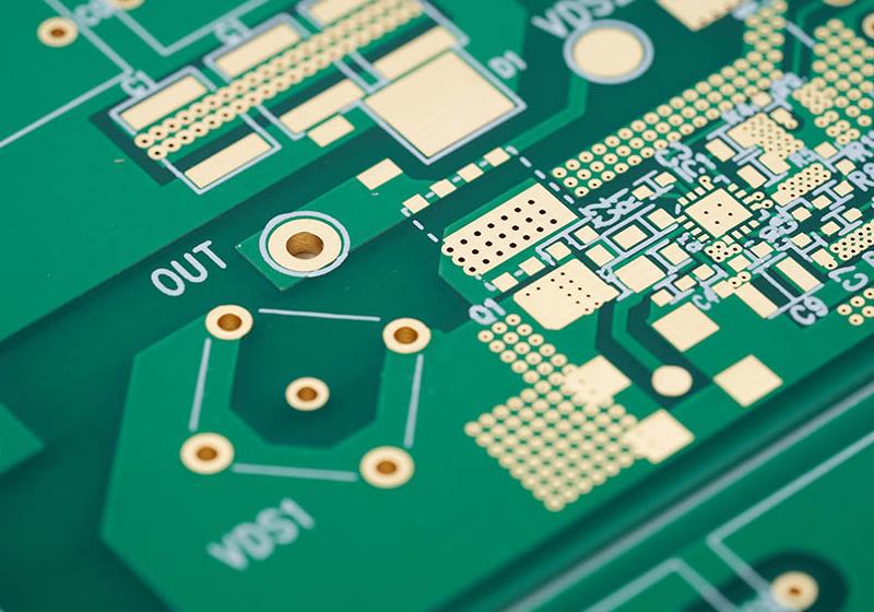
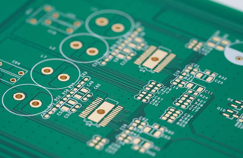
What is a PCB Gold Plating?PCB gold plating and gold plating pcb is a commonly used surface treatment process in PCB board production today. Simply put, Immersion gold is a chemical deposition method, through the chemical oxidation reduction reaction on the surface of the PCB board to produce a layer of metal plating, to prevent the board surface PAD oxidation.
The copper on the PCB board is mainly copper violet, copper solder joints in the air is easy to be oxidised, which will result in conductivity, that is, eat tin poor or poor contact, reducing the performance of the PCB board.
Then the need for surface treatment of copper solder joints, gold is sunk on top of the PAD layer of gold, gold can effectively block the copper metal and air to prevent oxidation, so the gold is the surface of the anti-oxidation of a processing pipeline, is through a chemical reaction on the surface of copper covered with a layer of gold, also known as immersion gold at the same time.
The first step in the PCB surface treatment process is to carefully clean the uncovered copper after applying the soldering cap.After cleaning any deteriorated copper,the PCB fabricator uses micro-etching to create the surface structure ready for the Pd catalyst.The PCB manufacturer then adds the catalyst by washing the PCB in a palladium sulphate solution.After applying the palladium,the circuit board manufacturer carries out another cleaning of the PCB and then places it in a nickel phosphate layered bath,which deposits a layer of metallic nickel on top of the catalytic copper.After cleaning,the PCB is immersed in a gold bath of potassium gold cyanide and gold salts to make the metal adhere to the nickel plating layer.

PCB gold plating
What are the features of gold plated PCB?
1.Gold plated PCBs have bright colours, good luster and good appearance.
2.The crystal structure formed by gold plating is easier to solder than other surface treatments, and can have better performance and quality assurance.
3.Because the gold plating only has nickel gold on the pads,it will not affect the signal,because the signal transmission in the skin effect is in the copper layer.
4.The metal content of gold is more stable,the crystal structure is more dense,and oxidation is not easy to occur.
5.Because only the soldering pads on the gold plated board have nickel gold,the solder resist on the line is more firmly bonded with the copper layer, and it is not easy to cause micro-short circuits.
6.The project will not affect the spacing when making compensation.
7.The stress of the board is easier to control.

Chemical Gold PCB
As a circuit board manufacturer specialising in high-end PCBs,Abbey Circuits has provided customised services to a number of well-known companies.Please contact us for customised PCB boards.