Preparation before circuit card assembly
• DFM check
Before the actual assembly process, the PCB design should be thoroughly checked to fully understand the functionality and manufacturability of the board. This stage helps to check for design errors and allows designers to eliminate all defects for successful production.
• Incoming quality control (IQC)
The manufacturer must check whether the incoming components are correct and the shape is normal (whether there is deformation, broken pins, oxidation, etc.) according to the part number and quantity of the BOM list, especially IC chips or other complex and expensive components. In addition, the manufacturer will also use tools such as test fixtures and multimeters to perform spot tests or full tests on the incoming components. If defects are found or they do not match the BOM list, all components will be returned to the component supplier or customer.
• Machine data programming
After receiving the bare PCB board and all components, the next step is to set up and program all the machines required in the PCBA process flow. SMT machines, AOI (automatic optical inspection) machines, and other machines need to set up programs. For example, SMT placement machines need to be programmed to accurately mount components, and this program is best generated by CAD data, but it often does not work properly. Always use the Gerber file as this is what is required to manufacture the bare PCB.
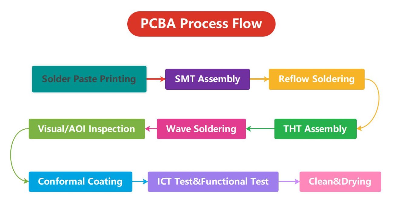
Circuit card assembly Process Flow – Step by Step Guide
1. Solder Paste Printing
Solder paste printing is the first step in the printed circuit board assembly process and involves using a stencil to apply the required amount of solder paste to the PCB surface accurately so that the components can be properly soldered to the board.
The size of the stencil must be exactly the same as the size of the board and the type of solder paste must also match the soldered components. The solder paste is then applied to the designated pads of the PCB using a scraper or knife blade to ensure an even coating.

2. SMD Assembly
After the solder paste is printed on the PCB surface, the next step is component placement. In the past, the picking and placement of components, such as surface mount components, used to be done manually.
Now, machines pick up and accurately place components in pre-planned areas of the board. Each component is then taken out of the component package by a vacuum nozzle or a fixture nozzle, inspected by the system, and placed at the programmed location at high speed.
3. Reflow Oven
After the PCB components and solder paste are in place, they must adhere properly. For this reason, solidification is necessary to connect the parts to the board via reflow. Most PCBAs require special considerations during the reflow process, more so for double-sided PCB assembly.
4. Inspection after reflow
When these components are soldered in place, the board needs to be tested to determine its functionality. During the reflow process, movement can result in missing or poor connections. Inspection and quality control can be done manually or automatically. Despite smart and automated manufacturing, you still need manual inspection on the SMT side). This will allow the pick and place machines to easily pick and place components on the PCB (regularly for PCB assembly)
Unfortunately, manual assembly tends to be inaccurate. Automated optical inspection is more suitable for large volumes. Here, PCB manufacturers use automated machines to process large numbers of PCBs in a short period of time.
Finally, X-ray inspection is performed. This type of inspection method is not common, although it is heavily used in complex and layered PCBs. Using X-rays, the observer can see through the layers and then visualize the lower layers to see hidden problems.
5. THT Assembly
Some types of components need to be inserted into the PCB board, which is usually done manually.
6. Wave Soldering
After the PTH components are inserted into the PCB and inspected, we will solder the components through wave soldering. Wave soldering is a large-scale soldering process that involves soldering electronic components to the PCB to form an electronic assembly. The name comes from the waves that use molten solder to connect metal parts to the printed circuit board.
7. Visual/AOI Inspection
Inspections after wave soldering include visual inspection, AOI inspection, and tests to measure electrical characteristics such as continuity, voltage drop, and resistance. By performing these inspections regularly, manufacturers can ensure that their products will function properly after use.
8. Conformal Coating
Some customers will require conformal coating for the finished PCBA. Conformal coating is a protective non-conductive dielectric layer on the printed circuit board assembly. Its function is to protect the circuit board and prevent the components from being corroded by pollution, salt spray, humidity, fungus, dust, and harsh or extreme environments.
Conformal coating is a critical step in the PCB assembly process because it helps protect the board from environmental factors and static electricity. In addition, using the right coating material in the PCB assembly process steps helps ensure the quality and reliability of the final product, saving time and money in the long run.
9. ICT Testing and Functional Testing
ICT testing may require electronic connection testing to ensure that the components are soldered correctly. If the customer requires functional testing, the test methods, test software and tools are usually provided by the customer, and we can also make test fixtures according to customer requirements.
10. Cleaning and Drying
The production process is relatively messy, and the solder paste will have some flux residue, so before sending the board to the customer, the surface oil must be thoroughly cleaned. First, use PCB cleaning in deionized water or ultrasonic cleaning. After cleaning, use compressed air to completely dry the PCB.
The above is the general process of circuit board assembly. In actual assembly, it will be more complicated and encounter many problems, but as an experienced PCB assembly supplier, all problems are minor problems for us.