A Trustworthy PCB and Electronic Manufacturing Enterprise! Contact Us


The rapid development of the electronic information industry has led to the development of electronic products in the direction of miniaturization, functionality, high performance, and high reliability. From general surface mount technology (SMT) in the mid-1970s to high-density interconnect surface mount technology (HDI) in the 1990s, as well as the application of various new packaging technologies such as transistor packaging and IC packaging technology in recent years, electronic mounting technology Continuously develop towards high density. At the same time, the development of high-density interconnection technology promotes the development of PCBs in the direction of high density. With the development of mounting technology and PCB technology, the technology of copper clad laminate as PCB substrate material is also constantly improving.
Copper Clad Laminate (CCL), as the substrate material in PCB manufacturing, mainly plays the role of interconnection, insulation and support for PCB, and has a great impact on the signal transmission rate, energy loss and characteristic impedance of PCB. circuit. Therefore, the performance, quality, manufacturing technology, manufacturing level, manufacturing cost, and long-term reliability and stability of PCB copper clad laminates largely depend on the material of the copper clad laminate.
CCL technology and production have experienced more than half a century of development. Now the global annual output of copper-clad laminates has exceeded 300 million square meters, and copper-clad laminates have become an important part of the basic material of electronic information products. The copper clad laminate manufacturing industry is an emerging industry. With the development of electronic information and communication industry, it has broad prospects. Its manufacturing technology is a high-tech that crosses, penetrates and promotes multiple disciplines. The development history of electronic information technology shows that copper clad laminate technology is one of the key technologies that promotes the rapid development of the electronics industry.
The key tasks of the future development strategy of China's copper clad laminate (CCL) industry. In terms of products, we must work hard on the five types of new PCB substrate materials, that is, through the development and scientific and technological breakthroughs of the five types of new substrate materials. , which has improved the cutting-edge technology of China's copper-clad laminates. The development of the five types of new high-performance copper-clad laminate products listed below is a topic that engineering and technical personnel in China's copper-clad laminate industry should focus on in future research and development.

Developing lead-free copper clad laminates is crucial for compliance with EU directives like WEEE and RoHS, which prohibit the use of lead-containing materials in electronics. High-performance copper clad laminates include types like low-dielectric constant, high-frequency/high-speed, and high-heat-resistant laminates, essential for advanced PCB applications. Future development aims to meet increasingly stringent performance requirements aligned with evolving electronic assembly technologies by 2010.
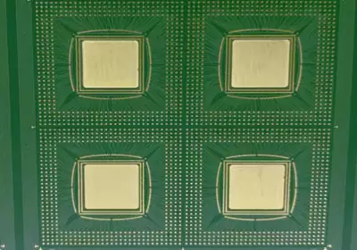
PCB substrate material-IC package carrier substrate material
The IC packaging carrier also needs to solve the problem of inconsistent thermal expansion coefficient with the transistor chip. Even for build-up multilayer boards suitable for making micro circuits, the thermal expansion coefficient of the insulating substrate is generally too large (generally the thermal expansion coefficient is 60ppm/℃). The thermal expansion coefficient of the substrate reaches about 6ppm, which is close to the thermal expansion coefficient of the transistor chip. This is indeed a "difficult challenge" for the substrate manufacturing technology.
In order to adapt to high-speed development, the dielectric constant of the substrate should reach 2.0, and the dielectric loss factor can be close to 0.001. For this reason, it is expected that around 2005, a new generation of printed circuits board will appear in the world that transcend the boundaries of traditional substrate materials and traditional manufacturing technologies.
In order to predict the future development of IC packaging design and manufacturing technology, there are stricter requirements for the substrate materials used. This is mainly manifested in the following aspects:
1. High Tg corresponding to lead-free solder.
2. Achieve low dielectric loss factor matching the characteristic impedance.
3. The dielectric constant corresponding to high speed (ε should be close to 2).
4. Low warpage (improving the flatness of the substrate surface).
5. Low moisture absorption rate.
6. The thermal expansion coefficient is low, making the thermal expansion coefficient close to 6ppm.
7. IC packaging carrier cost is low.
8. Low-cost substrate material with built-in components.
9. In order to improve the thermal shock resistance, the basic mechanical strength is improved. Suitable for substrate materials that do not reduce performance under temperature change cycles from high to low.
10. Achieve low cost and green substrate material suitable for high reflow soldering temperature.
D. PCB substrate material is copper-clad laminate with special functions
The copper-clad laminates with special functions mentioned here mainly refer to: metal-based (core) copper-clad laminates, ceramic-based copper-clad laminates, high dielectric constant laminates, copper-clad laminates (or substrate materials) for embedded passive components - many types Laminates, copper clad laminates for photoelectric circuit subatrate, etc. The development and production of this type of copper-clad laminate is not only a need for the development of new technologies for electronic information products, but also for China's aerospace and military industries.
PCB substrate material high performance flexible copper clad laminate
Since the large-scale industrial production of flexible printed circuit boards (FPC), it has experienced more than 30 years of development. In the 1970s, FPC began to enter real industrial mass production. In the late 1980s, due to the emergence and application of a new type of polyimide film material, FPC became adhesive-free FPC (generally referred to as "two-layer FPC"). In the 1990s, the world developed photosensitive cover films corresponding to high-density circuits, which caused major changes in FPC design. Due to the development of new application areas, the concept of its product form has undergone many changes and has been expanded to include a wider range of TAB and COB substrates. The high-density FPC that appeared in the second half of the 1990s began to enter large-scale industrial production. Its circuit patterns quickly evolved to more subtle levels. The market demand for high-density FPC is also growing rapidly.
At present, the annual output value of FPC produced globally has reached approximately US$3 billion to US$3.5 billion. In recent years, global FPC production has continued to increase. Its proportion in PCB is also increasing year by year. In countries such as the United States, FPC accounts for 13%-16% of the entire printed circuit board output value. FPC is increasingly becoming a very important and indispensable variety in PCB.
In terms of flexible copper-clad laminates, there is a large gap between China and advanced countries and regions in terms of production scale, manufacturing technology level, and raw material manufacturing technology. This gap is even larger than that of rigid copper-clad laminates.