1. Introduction
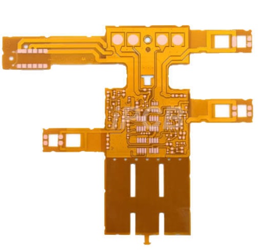
Flexible Printed Circuit Boards play an indispensable role in modern electronic devices due to their lightweight, thin profile, and bendable nature, which enable efficient space utilization. Coverlay Flex PCB, a key type of FPCB, utilizes a coverlay film to protect copper traces and dielectric layers while ensuring stability under repeated bending, stretching, and high-temperature environments. With the development of consumer electronics, automotive electronics, medical devices, and aerospace applications, FPCBs face increasingly stringent requirements for reliability, miniaturization, high-frequency performance, and process precision.
2. Materials and Structure
The performance of Coverlay Flex PCB is determined by its material composition and layer structure. Typical stack-up includes:
Copper Foil (Conductor Layer): Standard thickness ranges from 9–35 μm and can be adjusted according to current carrying requirements. Thick copper foils are applied in high-power or thermal management scenarios. Surface treatments such as oxide, ENIG (Electroless Nickel Immersion Gold), or OSP (Organic Solderability Preservatives) are commonly used to enhance solderability and prevent oxidation.
Polyimide (PI) Film: Thickness typically ranges from 25–125 μm, with high thermal stability up to 260°C. PI film provides excellent flexibility and electrical insulation.
Adhesive Layer: Bonds the PI film to copper traces, ensuring stable performance under thermal cycling, bending, or vibration.
Multilayer Designs: Coverlay Flex PCB can consist of 2–10 circuit layers for high-density and miniaturized designs. The stack-up sequence, trace spacing, and dielectric thickness must be carefully engineered to ensure signal integrity and voltage withstand capability.
3. Manufacturing Process and Key Control Points
The manufacturing process of Coverlay Flex PCB directly affects bending lifetime, signal stability, and production yield. Core processes include:
1.Coverlay Lamination:
PI film is laminated onto copper traces through heat and vacuum pressing.
Temperature and pressure control are critical; excessive heat may cause bubbles or warping, while insufficient heat can lead to delamination.
2.Coverlay Opening:
Windows are created at pads or test points using photolithography or laser cutting to allow component soldering.
Laser cutting precision can reach ±25 μm, suitable for high-density designs.
3.Trace Fabrication and Surface Treatment:
Copper traces can be thickened (18–70 μm) or designed for fine pitch (≥50 μm spacing).
Surface finishes (ENIG, immersion tin, OSP) are selected according to soldering and reliability requirements.
4.Quality Control and Performance Verification:
Bend Life Testing: ≥10,000 bending cycles at 3–5 mm bend radius.
Thermal Cycling: -40°C to 150°C to check delamination and open circuits.
Electrical Performance: Dielectric constant εr ≈ 3.2, dielectric strength 50–100 V/μm, high-speed signal loss ≤3 dB.
5.Design Optimization Recommendations:
Minimize trace crossings and thick copper in bending regions.
High-frequency traces should be placed near the neutral axis to reduce stress.
For thick copper or multilayer boards, use flexible vias or thinning zones to improve bendability.

4. Performance Metrics and Validation Data
In a smartwatch project, a Coverlay Flex PCB with 50 μm PI film and 18 μm copper foil maintained only 0.05% resistance variation after 10,000 bending cycles at 3 mm bend radius, with S-parameter testing showing <2 dB high-frequency signal attenuation.
For automotive sensor flex boards, 75 μm PI film combined with 35 μm thick copper passed 100 cycles of thermal cycling (-40°C to 150°C) and vibration testing, with no delamination or cracking, meeting IPC-6013/IPC-6012 Class 3A standards.
In high-frequency RF applications, 0.15 mm trace width and spacing multilayer boards achieved signal loss <0.5 dB/cm at 10 GHz, ensuring stable high-speed transmission.
5. Application Examples
1.Consumer Electronics: Smartwatches, foldable smartphones, tablets – requiring high bend life and ultra-thin design.
2.Automotive Electronics: Instrument clusters, cameras, and sensors – demanding high-temperature, vibration, and humidity resistance.
3.Medical Devices: Implantable and portable monitoring devices – requiring flexibility, thinness, and high reliability.
4.Aerospace and Industrial: UAV control boards, aerospace electronics – high reliability compliant with IPC Class 3A or IPC-6012DS standards.
5.High-Frequency Communication: Antenna modules, RF boards, and 5G communication terminals – requiring low dielectric loss, precise impedance control, and high-speed signal stability.
6. Conclusion and Future Trends
Coverlay Flex PCB, with its high flexibility, reliability, and multi-layer stack-up capabilities, is widely applied across consumer electronics, automotive, medical, and aerospace industries. Future trends include:
•Ultra-Thin and Miniaturized Designs: PI film thickness reduced to 12–25 μm for extreme space constraints.
•Low-Loss Materials: Supporting high-frequency and millimeter-wave applications.
•Laser Precision Processing: Enhancing coverlay window accuracy and multilayer alignment for high-density designs.
•Thick Copper and Multilayer Optimization: Balancing current carrying capacity with flexible bendability.
•Smart Manufacturing: Integrating AOI (Automated Optical Inspection) and bend-life prediction models to further improve reliability and production efficiency.
Coverlay Flex PCB technology continues to evolve toward higher frequencies, higher density, and extreme environment resilience, solidifying its position as a core enabling technology in modern electronics design.