Designing your own PCB from a piece of raw material is an exciting and creative project, transforming theoretical electronic concepts into a physical surface. Whether for hobby or practical purposes as an engineer, the ability to create a pcb board is a valuable asset.
A PCB can be defined as the fundamental component of most devices, providing not only the mechanical foundation for mounted components but also establishing and transmitting electrical connections between them. So, let's take a look at how to design a PCB in 10 steps.
If you've been doing this for decades, you don't need to tell you how valuable understanding design software is for properly designing PCBs. Without accurate and reliable integration from schematic capture to layout, laying out traces for wiring and copper traces or managing the layers required for solder can be challenging.
Step 1: Create a Schematic
Whether you're generating a design from a template or create a pcb board from scratch, you start with a schematic. A schematic is like a blueprint for a new device, and understanding what's shown in it is crucial. First, the schematic shows you:
What components are used in the design
How the components connect together
The relationships between component groups in different schematics
This last point is crucial, as complex designs may utilize layered schematics. If you design using a layered approach and place different circuit blocks in separate schematics, you can significantly enhance organization within your new board. Not only are circuit interconnections easier to define and edit than designing directly on the board, but converting the schematic to a board layout is also much easier. For components, PCB design software often features extensive part library databases.

Step 2: Create a Blank PCB Layout
After creating the schematic, you need to use the schematic capture tools within your PCB design software to begin creating the PCB layout. Before doing this, you need to create a blank PCB document. Creating a board requires generating a PcbDoc file. This can be easily done from the design software's main menu.
If you've already determined the PCB shape, dimensions, and layer stackup for your board, you can set these up immediately.
Step 3: Schematic Capture: Linking to the PCB
All tools within PCB design software work within a unified design environment, where the schematic, PCB, and BOM are interconnected and accessible simultaneously. Other programs force you to manually compile schematic data.
Step 4: Design the PCB Stackup
When you transfer your schematic information to PcbDoc, the component footprints are displayed in addition to the specified board outline. Before placing components, you should define the PCB layout (i.e., shape, layer stackup) using the Layer Stack Manager, as shown below.
If you're new to PCB design, while you can define any number of layers in your PCB design software, most modern designs will start with a 4-layer board on FR4. You can also take advantage of the Material Stack Library, which allows you to choose from a variety of different laminates and unique board materials.
If you're designing for high speed/high frequency, you can use the built-in impedance analyzer to ensure impedance control in your board. The Impedance Profile tool uses Simberian's integrated electromagnetic field solver to customize trace geometry to achieve target impedance values.

Step 5: Define Design Rules and Design-For-Function (DFM) Requirements
There are many categories of PCB design rules, and you may not need to use all of them for every design. Rules used for manufacturing should meet the specifications and tolerances of the PCB manufacturer's equipment. Advanced designs, such as impedance-controlled designs and many high-speed/high-frequency designs, may require very specific design rules to ensure proper function. Always check your component datasheets for these design rules.
Step 6: Place Components
Current mainstream PCB design software offers a lot of flexibility and allows you to quickly place components on the board. Components can be arranged automatically or placed manually. You can also use these options together, taking advantage of the speed of automatic placement while ensuring that the board is laid out following good component placement guidelines.
Step 7: Insert Drill Holes
Drill holes (mounting and vias) are placed before routing. If the design is complex, you may need to modify at least some of the via locations during the trace routing process. The design for manufacturing (DFM) specifications from the PCB manufacturer should be followed here.
Step 8: Route Traces
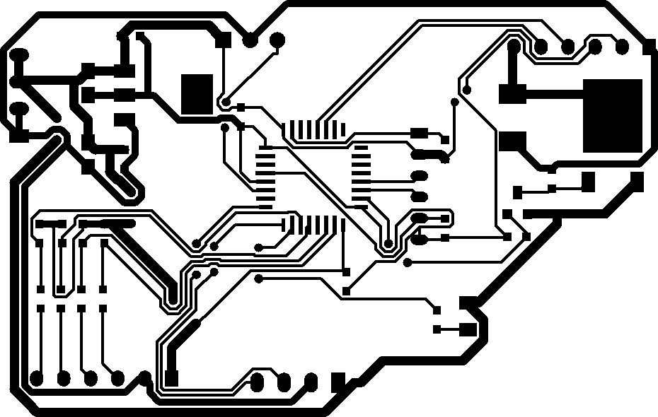
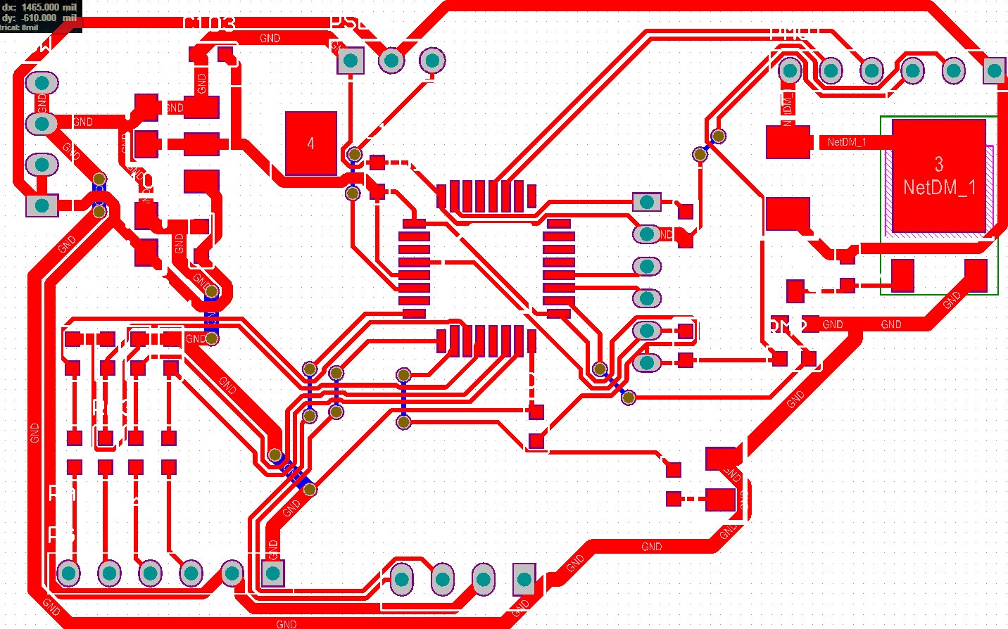
After placing the components and any other mechanical elements, you are ready to route the traces. Be sure to use good routing guidelines and utilize PCB design software tools to simplify the process, such as net highlighting and color coding by routing.

Step 9: Add Labels and Identifiers
After verifying the board layout, you can add labels, identifiers, markings, logos, or any other images to the board. It is a good idea to use reference identifiers for components, as this will aid in PCB assembly. Also, include polarity indicators, pin 1 indicators, and any other labels that help identify the component and its orientation. For logos and images, consult iPCB to ensure the fonts you use are readable. Step 10: Generate Design Gerber Files
Before creating manufacturer deliverables, always verify your board layout by running a design rule check (DRC). After your board passes the final DRC, you need to generate design files for your manufacturer. The design files should include all the information and data needed to build the board; include any comments or special requirements to ensure your manufacturer understands your requirements. For most manufacturers, you'll have access to Gerber files.
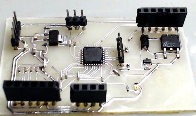
With these ten steps, you're ready to create a pcb board. Give it a try!