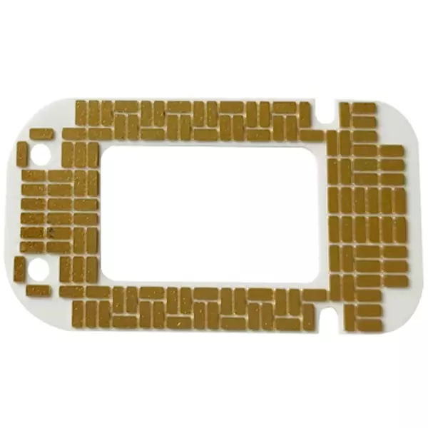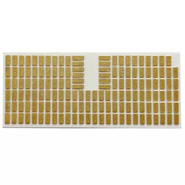

Substrate thickness: 1.0mm
Layers: 1L
Substrate: 96% alumina ceramic base
Thermal conductivity: 30W
Surface technology: ENIG
Copper thickness: 300um
Manufacturing process: DBC Ceramic
DBC (Direct Bonded Copper) direct copper deposition technology uses an oxygen-containing eutectic solution of copper to directly deposit copper onto ceramics. The basic principle is to introduce an appropriate amount of oxygen element between copper and ceramics before or during the deposition process. Within the range of 1065 ℃~1083 ℃, copper and oxygen form a Cu-O eutectic solution. DBC technology uses this eutectic solution to chemically react with the ceramic substrate to form CuAlO2 or CuAl2O4 phases, and to infiltrate the copper foil to achieve the bonding between the ceramic PCB and the copper foil. Mainly used in power semiconductor module packaging, refrigeration, and high-temperature gaskets.
DBC ceramic PCB is a ceramic surface metallization technology, and DBC substrates mainly consist of two materials: Al2O3 ceramic substrates and AlN ceramic substrates. The surface metallization techniques for alumina and aluminum nitride ceramic substrates are roughly the same. Taking Al2O3 ceramic substrate as an example, by heating the ceramic substrate in an oxygen-containing nitrogen N2 atmosphere, copper Cu foil is directly soldered onto the Al2O3 substrate.
In the process of ceramic surface metallization, the Cu2O eutectic liquid phase formed by Cu atoms and O atoms wets the Cu foil and Al2O3 ceramic surfaces in contact with each other, and also reacts with Al2O3 to generate composite oxides such as Cu (AlO2) 2 and Cu (AlO2), which serve as solder for eutectic brazing and firmly bond the two together. AlN ceramic substrate is a non oxide ceramic, and the key to bonding copper foil is to form a transition layer on its surface that meets the above bonding conditions. The mechanism of covering copper foil on the transition layer is roughly the same as that of Al2O3 ceramic substrate.

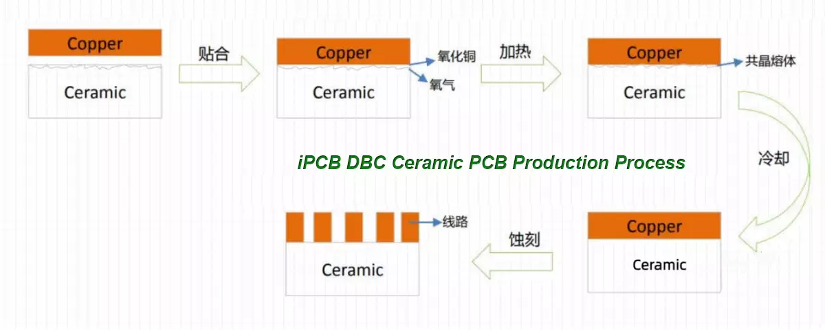
DBC Ceramic PCB Production Process
DBC ceramic PCB is mainly used as a carrier for various chips (IGBT chips, diode chips, resistors, SiC chips, etc.) in power electronics module technology. DBC ceramic PCB completes the connection of chip connection poles or surfaces through surface copper coating, and its function is similar to PCB board. DBC ceramic PCB has significant characteristics such as good insulation performance, good heat dissipation performance, low thermal resistance coefficient, matched expansion coefficient, excellent mechanical performance, and good soldering performance.
1. Good insulation performance
Using DBC substrate as the carrier of the chip can effectively isolate the chip from the module heat dissipation bottom plate. The Al2O3 ceramic layer or AlN ceramic layer in the middle of the DBC substrate can effectively improve the insulation ability of the module (ceramic layer insulation withstand voltage>2.5KV).
2. Excellent thermal conductivity
The DBC substrate has good thermal conductivity, with a thermal conductivity of 20-260W/mK. During the operation of IGBT modules, a large amount of heat is generated on the chip surface, which can be effectively transmitted to the module's heat dissipation base plate through the DBC substrate, and then conducted to the heat sink through the thermal grease on the base plate, completing the overall heat dissipation flow of the module.
3. The expansion coefficient of DBC ceramic PCB is close to that of the chip
The expansion coefficient of DBC substrate is similar to that of silicon (the main material of the chip is silicon) (7.1ppm/K), which will not cause stress damage to the chip. DBC substrate has a peel resistance of>20N/mm2, excellent mechanical properties, corrosion resistance, and is not easily deformed, and can be used in a wide temperature range.
4. The welding performance of DBC ceramic PCB is good
The DBC substrate has good welding performance, with a welding void rate of less than 5%. The DBC substrate has a thick copper layer that can withstand high current loads. Under the same cross-section, it only requires 12% of the conductive width of a typical PCB board, and can transmit greater power per unit volume, improving the reliability of the system and equipment. It is precisely because of the various excellent properties of DBC substrates that they are widely used in the preparation of various types of high-power semiconductors, especially IGBT packaging materials.
The main process flow of DBC ceramic PCB
Cleaning and drying of ceramic substrates and copper foils → copper foil pretreatment → high-temperature eutectic bonding of copper foil and ceramic substrates → cold and hot step cycle cooling → quality inspection → etching of patterns as required → chemical nickel (or gold) plating → quality inspection → laser cutting and cutting → finished product quality inspection → vacuum or nitrogen filled packaging → entering the finished product warehouse.
The meaning of DBC ceramic PCB is that ceramic powders such as alumina, aluminum nitride, or doped zirconia are cast and sintered into ceramic PCB substrate, and then metalized to prepare ceramic copper-clad laminates. DBC ceramic PCB has good stability, high current carrying capacity, high electrical insulation, and high thermal conductivity.
DBC ceramic PCB is a metalized substrate formed by directly sintering copper onto alumina or aluminum nitride ceramics under high temperature conditions. The application fields are quite extensive, including the LED intelligent lighting industry, power electronic device industry, etc. It also undertakes the important tasks of high current carrying capacity and heat dissipation for power electronic component carrier boards in the automotive grade IGBT modules of the new energy vehicle industry.
DBC is just one way of making ceramic PCB into ceramic copper-clad substrate, in addition to DPC ceramic PCB, AMB ceramic PCB, LAM ceramic PCB, etc.
The DBC direct bonding copper process utilizes high-temperature heating to combine aluminum oxide (AI ²O³) with copper (Cu) plates. However, even though DBC ceramic PCB is a cutting-edge mass production technology in the industry, tiny bubbles are inevitably present on the bonding surface. The heat generated during the use of DBC ceramic PCB can further expand the bubbles, ultimately leading to product failure.
Substrate thickness: 1.0mm
Layers: 1L
Substrate: 96% alumina ceramic base
Thermal conductivity: 30W
Surface technology: ENIG
Copper thickness: 300um
Manufacturing process: DBC Ceramic
iPCB Circuit provides support for PCB design, PCB technology, and PCBA assembly. You can request technical consultation or quotation for PCB and PCBA here, please contact email: sales@ipcb.com
We will respond very quickly.