A Trustworthy PCB and Electronic Manufacturing Enterprise! Contact Us


In the production of electronic products, PCB boards and ICs are important components. IC integrates a general circuit onto a chip. It is a whole. Once it is damaged internally, the chip will also be damaged. PCB components can be soldered by oneself, and components can be replaced if they break.
The manufacturing process of IC is to interconnect the transistors, resistors, capacitors, inductors and other components and wiring required in a circuit, and make them on one or several small transistor wafers or dielectric substrates, and then package them in a Inside the tube shell, it finally becomes a microstructure with the required circuit functions.
The IC carrier board is generally the carrier board on the chip. The board is very small, usually about the size of 1/4 fingernail, and the board is very thin 0.2~0. 4mm, the material used is FR-5, BT resin, and the circuit is about 2mil/2mil. It is a high-precision board. The unit price of this board is very high, and it is usually purchased on a PCS basis.

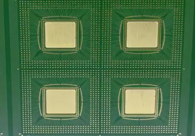
IC carrier board and PCB board
PCB board is the PCB substrate for our mobile phones, computers and peripherals. There are Note-BOOK boards, memory strips, LCD, HDI boards. PCB boards are generally around 1.0-1.6MM, and the lines are 4mil/4mil to 2mil/2mil. FR is mostly used for materials. -4 Epoxy resin is now a commodity and is generally sold by area. The yield rate is generally above 90%. If the yield rate is lower than this, there is a possibility of losing money. Generally, a good PCB board factory can achieve 98%.
From the appearance point of view, the background color of the PCB board is usually green, but it is not limited to green. The background color of this layer mainly depends on the color of the solder mask ink used in the solder mask layer. There is also a screen printing surface printed on the solder mask layer, usually with text and symbols on it to identify the location of the part.
Using PCB boards as components has the following main advantages: reducing wiring and assembly errors, conducive to circuit interchange, conducive to miniaturization of electronic equipment, and conducive to mechanization and automation of equipment production.
PCB boards can be classified into single-sided boards, double-sided boards, and multi-layer boards. Multi-layer boards include HDI boards (high-density connection boards), flexible boards, and rigid-flex boards. Continuing development from high-density connection boards, SLP (carrier type PCB board) is formed. Its width and distance limit requirements are higher than those of HDI boards, and the more difficult category is IC boards.
Classification from technical parameters: IC carrier board has 2-10 layers, class carrier board also has 2-10 layers, HDI board has 4-16 layers, and ordinary PCB board can have more than 100 layers. There are also differences in board thickness between different categories. IC carrier boards are the thinnest, usually within 1.5mm, and can be as thin as 0.1mm. SLP is thicker than IC, HDI is thicker than HLP, and the thickest PCB board is more than 7mm. . The most important parameter is line width and line spacing (width and spacing of internal lines). IC carrier boards are approximately within 25um (1mil), class carrier boards are more than 1mil, HDI is about 2mil, and ordinary PCBs are more than 2mil.
From a process perspective: PCB is made using the subtractive method (the copper foil is exposed and etched to leave the lines), while the IC carrier board is made using the additive method because its line width and line spacing are extremely small (chemicals cannot be used). The similar carrier board uses an improved additive method, citing the subtractive method process and adding a partial additive method.
From an application perspective: communications account for one-third, computer PCB applications account for 20%, consumer electronics account for 15%, transistors account for 10%-20%, automobiles account for less than 10%, and the remaining part is medical. The overall proportion of communications and computers exceeds 50%. The market size of the overall PCB industry in 2020 will be US$70 billion, with China accounting for about 70%. The annual compound growth rate from 2018 will be less than 5%, and some sub-sectors have grown significantly: IC carrier boards in the past two years The growth rate is as high as 25% and will drop to 10% in the future. The output value of low-end boards (single-panel and double-panel) has declined, by about 2%-3% per year, and HDI boards have grown by 10% per year, so the main The growth rate comes from IC carrier boards and HDI boards. The output value of multilayer boards has increased slightly, and soft boards (flexible boards) have also increased.
The output value of IC substrates will exceed 10 billion US dollars in 2020, and the annual compound growth rate is expected to be 10%. Technological differences mainly exist in line width and line spacing, which leads to different choices of subtractive method, additive method and improved layering method. Since the IC carrier board has high requirements on width and spacing, it is the most technologically difficult and the adaptation pipeline is also different. In the future, the requirements will be higher, and the line width and line spacing will reach 0.5nm. Line width and line spacing make the requirements for copper thickness, circuit uniformity, and consistency higher than ordinary PCB boards, so the requirements for manufacturing equipment and chemical control are different from ordinary PCB boards.
The base materials of IC carrier board are mainly ABF and BT. BT is a resin material with a usage rate of more than 90%. The other is ABF, which was discovered by Japan's Ajinomoto Company when manufacturing MSG and is very useful for IC production. Both BT and ABF are produced in Japan. Because BT's patent has expired, companies outside Japan have begun production, but the products produced by Japanese companies are of higher quality. ABF is entirely produced by Ajinomoto Company, and its products have higher ductility, consistency, and thickness than those of other companies in the same industry. In order to seize the market, Ajinomoto mass-produces products and reduces profits, which is very detrimental to other competitors. Therefore, ABF is produced by this company this year. Since many patents are public, ABF-related technologies can be mastered. If the Chinese government conducts research and development regardless of cost, basically the same products can be produced after 3-5 years of technological accumulation. There are few domestic companies that can produce IC carrier boards, and their output value accounts for about 50% of the world's. The main international players come from Taiwan, South Korea, and Japan.
The concentration of leading manufacturers of IC carrier board is high. Japan, Taiwan, South Korea, and the United States account for 15% of the world's production output value in mainland China, and domestic asset value accounts for 5%. The leading merchants account for nearly 40% of the output value. Therefore, the concentration of carrier boards is high. high. And the core data are all produced by Japanese companies, ABF is used by high-performance CPUs, Japan's Ajinomoto has a market share of over 99%+, and another Japanese company accounts for less than 1%. ABF data continues to be out of stock and is expected to improve by 2025. The equipment cycle of IC carrier boards is more than one year in both Japan and South Korea. Domestic demand is growing. Affected by machine materials and ABF, production capacity is released slowly, with an annual growth rate of about 10%-15%. Production started a year and a half later. There were two fires in Xinxing, and there was also a fire in IBIDEN in Japan. After several fires, the supply of IC substrates was unable to be met.
AbF mainly uses traditional equipment. The biggest risk is that it is unable to obtain sufficient data. Moreover, ABF is used for high-end chips and may be restricted by political influence. The risk point of ABF lies in the single source of supply and insufficient production capacity release.
In the next 2-3 years, vehicles and data centers will be downstream application areas that will increase rapidly. The driving force for IC carrier boards comes from the fields of communications, consumer electronics, new energy, and automobiles. For example, SLP is used in mobile phones. Apple started using SLP from Iphone X. Now the usage is gradually increasing. Samsung and Huawei have begun to introduce some SLP. This is mainly The pull comes from the CPU and GPU.
BT and ABF materials are completely different. BT is made of two polymer materials mixed together. ABF is made by Ajinomoto from Japan, the only one. BT currently has Mitsubishi, Panasonic, Nanya, etc. that can do it. 99%+ of ABF’s global products are made by one company.
In short, an IC is an integrated chip soldered on a PCB board, and the IC carrier board is the carrier of the IC.