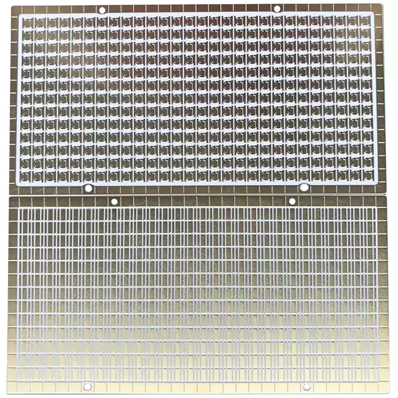
Substrate type: alumina ceramic
Substrate thickness: 0.5mm
Conductive layer: copper, nickel, gold
Metal layer thickness: 35μm
Surface treatment: ENIG
Metal: 1layer
Conductive hole: 0.3mm conductive hole
Line width: 0.1mm
Production process: DPC Ceramic
Application: LED Light
What is DPC Ceramic PCB? DPC Ceramic is based on thin film circuit technology, achieving ceramic surface metallization through magnetron sputtering, and achieving copper layer thickness greater than 10 microns through electroplating. PCB circuit boards are manufactured using the DPC (Direct Plating Copper) method.
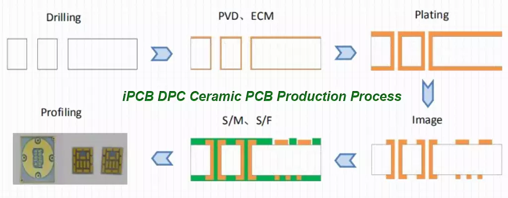
DPC mainly uses surface deposition processes such as evaporation and magnetron sputtering for surface metallization of circuit substrates. First, titanium is sputtered under vacuum conditions, then copper particles are added, and finally electroplating thickens. Then, circuit fabrication is completed using ordinary PCB processes, and finally, the thickness of the circuit is increased by electroplating/chemical plating deposition.
The manufacturing methods of DPC Ceramic PCB include vacuum coating, wet coating, exposure development, etching, and other process steps, so the price of DPC PCB is relatively high. The DPC process is suitable for most ceramic circuit board.
DPC ceramic PCB requires laser cutting to manufacture its shape, and traditional PCB drilling milling machines, and punching machines cannot accurately process it, so the bonding force and line width are also more precise. Metal has good crystallization performance, good flatness, less prone to circuit detachment, more accurate circuit positioning, smaller line spacing, and stable reliability.
DPC Ceramic PCB is the main component that serves as the underlying support structure for products in electronic devices. DPC Ceramic PCB is just one of many different types of ceramic circuit board that can be used to adapt to various working conditions.

DPC Ceramic PCB Production Process
Advantages of DPC Ceramic PCB
1. High thermal expansion effect
DPC Ceramic PCB is widely used in the electronics industry due to its high thermal expansion coefficient. This is because ceramic circuit boards can withstand high temperatures, and even when interacting with metals, the thermal conductivity of ceramic substrates is comparable to that of silicon. As is well known, they can serve as excellent isolation devices and perform exceptionally well for a considerable period of time. DPC Ceramic PCB maintains excellent thermal conductivity even at extremely high temperatures, paving the way for various new applications in various fields.
2. Multifunctionality
The application range of DPC Ceramic PCB is more comprehensive than other PCB because of their superior thermal expansion characteristics. This thin film copper-plated circuit board can be found in various applications. Ceramic circuit boards are the only choice in high-temperature environments, such as in some household appliances, which is necessary to ensure the continuous reliability of the circuit board over a period of time.
3. Good heat dissipation performance
In terms of heat dissipation, the use of ceramics on DPC Ceramic PCB will result in additional heat dissipation due to the presence of ceramic layers. In addition, DPC Ceramic PCB has a low coefficient of thermal expansion and high thermal conductivity, making it widely used.
The thin film copper-plated circuit board made of ceramic substrate becomes DPC Ceramic PCB. Another name for this type of circuit board is ceramic DPC and this special type of thin film coating
Substrate type: alumina ceramic
Substrate thickness: 0.5mm
Conductive layer: copper, nickel, gold
Metal layer thickness: 35μm
Surface treatment: ENIG
Metal: 1layer
Conductive hole: 0.3mm conductive hole
Line width: 0.1mm
Production process: DPC Ceramic
Application: LED Light
iPCB Circuit provides support for PCB design, PCB technology, and PCBA assembly. You can request technical consultation or quotation for PCB and PCBA here, please contact email: sales@ipcb.com
We will respond very quickly.