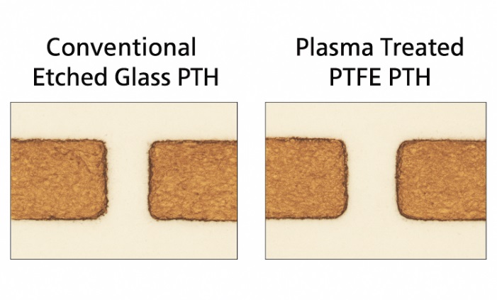
In high-frequency PCB manufacturing, PTFE (Polytetrafluoroethylene) materials are favored for their extremely low dielectric constant (Dk≈2.2) and dissipation factor (Df≈0.0009), making them ideal for radar, satellite communication, and RF modules.
However, the unique molecular structure and chemical inertness of PTFE pose major challenges in drilling and plated through-hole (PTH) metallization.
1. Characteristics of PTFE and Drilling Challenges
PTFE’s molecular chain contains numerous C–F bonds, giving it:
High flexibility (easy deformation)
Low surface energy (poor adhesion)
High melting point and thermal stability (difficult to cut mechanically)
During drilling, the following defects often occur:
Hole-edge burrs and tearing
Resin smearing or deformation on hole walls
Hole size deviation and residue clogging
If not properly managed, these defects lead to poor copper adhesion and reduced reliability.

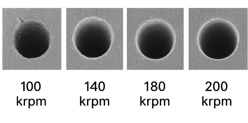
Microscopic comparison of PTFE hole walls at various drilling speeds (200× magnification)
2. Optimization of Drilling Parameters
Due to PTFE’s low hardness and high ductility, the drilling process must be carefully optimized.
1) Drill Bit Selection
Use sub-micron carbide drills for better precision;
Maintain a tip angle of 130°–140° to minimize smearing;
Apply TiAlN or DLC coating to improve durability and reduce friction.
2) Stack-Up Configuration
Use aluminum entry + paper exit pad to stabilize hole entrance and exit;
Limit each drilling stack to ≤2 panels to prevent heat accumulation.
3) Recommended Drilling Parameters
| Parameter | Suggested Range | Purpose |
| Spindle Speed | 120 – 180 krpm | High speed reduces burrs |
| Feed Rate | 25 – 50 µm/rev | Prevents elongation and deformation |
| Retract Speed | ≤300 mm/min | Avoids residue scratching |
| Pre-bake | 150°C × 2h |

Comparison of hole-wall smoothness at different spindle speeds (100–200 krpm)
3. Hole Wall Activation and Surface Treatment
Due to PTFE’s high chemical resistance, permanganate desmear is ineffective.
A plasma surface activation process is required to enhance adhesion for subsequent metallization.
Recommended Process Flow:
Low-temperature O₂/Ar plasma cleaning to remove carbonized layers
CF₄/He plasma modification to increase surface energy and wettability
Sn/Pd activation prior to electroless copper plating
After plasma treatment, surface energy improves by 2–3×, ensuring stronger copper adhesion.
4. PTH Metallization and Reliability Control
In PTFE PCBs, PTH copper must ensure both electrical continuity and thermal reliability.
Key control points:
Maintain electroless copper ≥0.3 µm for initial coverage
Control plating stress to match PTFE’s thermal expansion
Use neutral flexible additives to reduce internal stress
Validation Tests:
Inter-hole resistance & continuity testing
Thermal shock test (–40°C ↔ +125°C, 100 cycles)
Peel strength test (>1.0 N/mm)
5. Common Failures and Preventive Measures
| Failure Mode | Root Cause | Preventive Action |
| Copper peel-off | Insufficient activation | Extend plasma treatment or increase activation strength |
| Micro-cracks | Dull drill or low speed | Replace drills, increase rpm |
| Voids | Trapped gas | Apply vacuum plating, optimize degassing |
Drilling and metallization of PTFE high-frequency boards are among the most demanding processes in PCB fabrication.
They require precision equipment, tight process control, and a deep understanding of material behavior.
Through high-speed drilling, plasma activation, and low-stress electroplating,
manufacturers can significantly improve PTH reliability and signal consistency.
iPCB has developed mature drilling and metallization solutions for PTFE and hybrid high-frequency boards,
supporting Rogers RT/duroid, Taconic TLY, and Arlon 600 series materials.
For DFM evaluation or process validation on your specific PTFE design, contact the iPCB technical team.