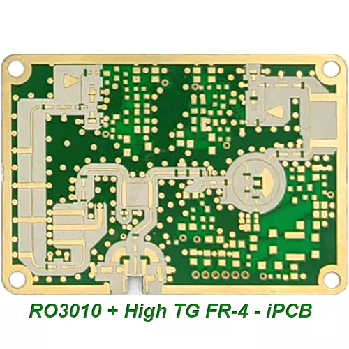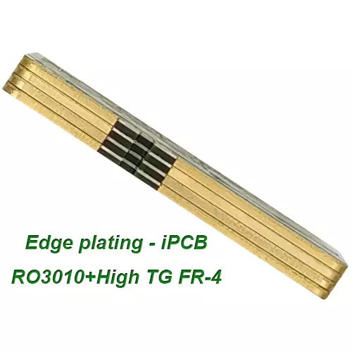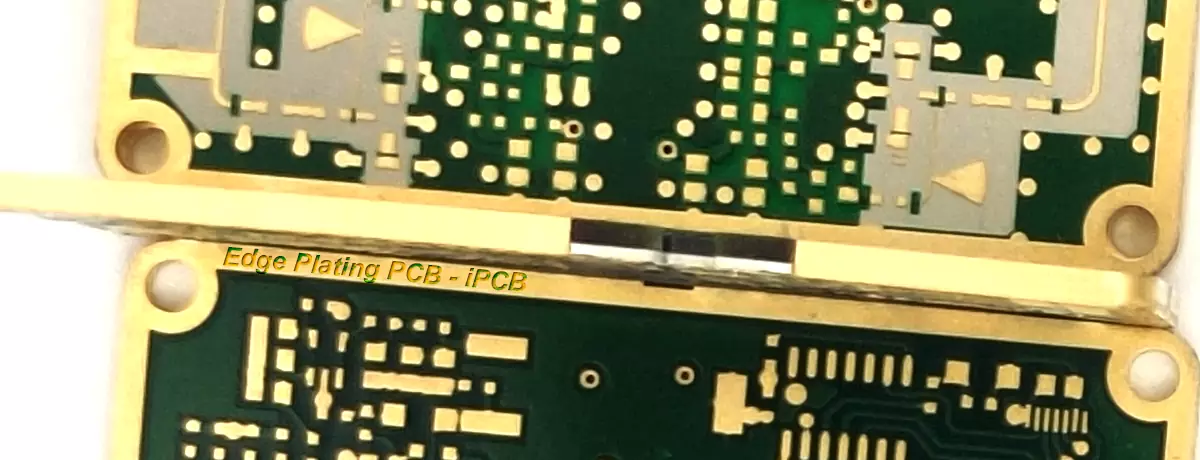

Product: Edge Plating PCB
Material: FR-4 or RF PCB
Layer: 2layer, multi-layer
Thickness: customizable
Copper thickness: 0.5oz-12oz
PCB thickness: 0.2-12mm
Solder mask colors: green, red, blue
Surface treatment: silver, glod
Special process: Edge Plating, mixed PCB
Application: communication, high-frequency
What is Edge Plating PCB?
Edge Plating PCB is a technology that processes a layer of metal at the edge of a circuit board to better secure and protect it. Metal edging is usually divided into two types: electroplated metal edging and non electroplated metal edging. Among them, electroplating metal edging requires first coating a layer of electroless copper plating on the circuit board, and then coating a layer of metal on it through electroplating. Commonly used metals include nickel, gold, silver, etc. Non electroplated metal edging is the process of directly pressing a layer of metal on the edge of a circuit board, commonly used metals include stainless steel, copper, aluminum, etc.
The metal edge wrapping process of PCB board, also known as edge electroplating or copper deposition edge wrapping process, is a technique for metalizing the board edges during the PCB manufacturing process. This process can significantly improve the performance and reliability of the circuit board by adding a layer of copper metal on the side of the PCB.
What is the function of Edge Plating PCB? Edge Plating PCB can enhance the mechanical strength of circuit boards and prevent them from breaking due to mechanical action. Metal edging can enhance the corrosion resistance of circuit boards and extend their service life. Metal edging can also reduce the electromagnetic radiation of circuit boards and improve their anti-interference ability.
In the actual production process, metal edging technology requires some preliminary preparations, such as selecting suitable metal materials and designing appropriate edging structures. Then, professional metal edging equipment such as metal presses, metal cutters, etc. need to be used for processing.
Edge Plating PCB process flow
Milling metal grooves: First, mill metal grooves on the side of the PCB Board to prepare for subsequent metallization treatment.
Chemical copper plating: Chemical copper plating is performed on the milled side to form a layer of copper skin.
Sinking gold treatment: Sinking gold treatment is performed on the surface of copper skin to provide better conductivity and oxidation resistance.
Surface treatment: Apply appropriate surface treatment to the edges after gold deposition to meet different application requirements.
What is a mixed PCB?
With the development of the electronics and communication industries, the design of high-frequency circuits and radio frequencies is becoming increasingly widespread. More and more high-frequency circuit board are being used on PCB to meet the requirements of signal transmission.
However, due to the high price of high-frequency board, from the perspective of cost saving, the structural design of PCB usually adopts a mixed pressing method of high-frequency circuit materials and FR-4. That is, except for the necessary signal layer using high-frequency copper-clad laminates to meet the requirements of signal transmission rate, signal integrity, and impedance matching, other layers still use conventional FR-4 materials, which are mixed pressing molded with high-frequency circuit materials.
The multilayer mixed high-frequency circuit board includes multiple insulating dielectric layers and multiple signal layers, where the dielectric layers and signal layers are alternately stacked.
The high-frequency signal layer includes a signal layer for transmitting high-speed signals and a signal layer for transmitting low-speed signals. The dielectric layer used for transmitting high-speed signals, which is stacked adjacent to the signal layer, uses high-frequency circuit materials, while other dielectric layers use second-class materials. Among them, the high-frequency characteristics of high-frequency circuit materials are better than those of FR-4 materials, and the dielectric loss caused by signal transmission is smaller than that of FR-4.
By mixing high-frequency low loss board with regular FR-4 board, multilayer circuit board can ensure good high-frequency performance while reducing manufacturing costs.
Mixed PCB is a type of PTFE mixed PCB, which is composed of layers of polytetrafluoroethylene fiberglass cloth and epoxy resin fiberglass cloth laminated together. The polytetrafluoroethylene fiberglass cloth layer has excellent high-frequency dielectric properties, high temperature resistance, and excellent radiation resistance, reducing the difficulty and cost of production processes. This structure of high-frequency mixed PCB can meet the requirements of local high-frequency signal transmission, while the cost of the entire mixed PCB precision circuit board itself is not high.
Mixed PCB requires the use of high-frequency circuit materials with different characteristics than traditional multilayer PCB board. The high-frequency mixed circuit board can be a mixture of FR4 and high-frequency PCB board, or a mixture of high-frequency board with different DK.

Edge Plating PCB
Why do some RF circuit boards require Edge Plating?
With the increase of system speed, not only the timing and signal integrity issues of high-speed signals become prominent, but also the EMC problems caused by electromagnetic interference and power integrity generated by high-speed digital signals in the system are also very prominent. The electromagnetic interference generated by high-speed digital signals not only causes serious mutual interference within the system, reducing its anti-interference ability, but also generates strong electromagnetic radiation to the outside space, causing the electromagnetic radiation emission of the system to exceed the EMC standard, making the products of circuit board manufacturers unable to pass EMC standard certification.
The edge radiation of multilayer PCB is a common source of electromagnetic radiation. When unexpected currents reach the edges of the ground and power layers, edge radiation occurs, resulting in insufficient power supply bypass and power noise. The cylindrical radiation magnetic field generated by the inductive via radiates between the layers of the circuit board and eventually converges at the edge of the circuit board. The reflux current of the strip line carrying high-frequency signals is too close to the edge of the circuit board. To prevent these situations from occurring, a circle of grounding vias is drilled around the PCB circuit board with a spacing of 1/20 wavelength holes to form a grounding via shield and prevent TME waves from radiating outward.
For microwave circuit boards, the wavelength is further reduced, and due to the current PCB production process, the spacing between holes cannot be made very small. At this point, the method of drilling shielding holes around the PCB with a spacing of 1/20 wavelength is no longer effective for microwave PCB boards. Therefore, it is necessary to use the Edge Plating process of the PCB board to surround the entire PCB board edge with metal, so that microwave signals cannot radiate from the PCB board edge. Of course, the production and manufacturing cost of using the Edge Plating PCB process increases significantly.
Product: Edge Plating PCB
Material: FR-4 or RF PCB
Layer: 2layer, multi-layer
Thickness: customizable
Copper thickness: 0.5oz-12oz
PCB thickness: 0.2-12mm
Solder mask colors: green, red, blue
Surface treatment: silver, glod
Special process: Edge Plating, mixed PCB
Application: communication, high-frequency
iPCB Circuit provides support for PCB design, PCB technology, and PCBA assembly. You can request technical consultation or quotation for PCB and PCBA here, please contact email: sales@ipcb.com
We will respond very quickly.