Factors affecting the quality of PCB soldering
From the PCB design, to all the components welded to become a high-quality PCB circuit board, PCB engineers, welding technology, welding workers and other aspects of control.
There are mainly the following factors: PCB drawings, the quality of the circuit board, the quality of the device, the oxidation of the device pins, the quality of the solder paste, the quality of the printing of the solder paste, the precise degree of the programming of the mounter, the quality of the paste machine, the paste quality of the reflow soldering furnace temperature curves and so on.
PCBA foundry itself can not overcome the link is the PCB drawing.
Circuit design engineers rarely welded circuit boards, can not get rich experience in welding, and PCBA foundry workers do not know how to draw the board, only to complete the production task, no mind, and even less capable of analyzing the causes of poor welding.
It is difficult to combine these two talents in their respective roles.
Suggestions when drawing PCBs
Below are some suggestions to avoid the emergence of a variety of bad welding quality affects the drawing.
1.PCB positioning holes to pay attention to the key points
PCB board to leave four holes in the corners (the smallest hole diameter 2.5mm), used to print solder paste when positioning the circuit board. Requirements for the X-axis or Y-axis direction of the center of the circle in the same axis.
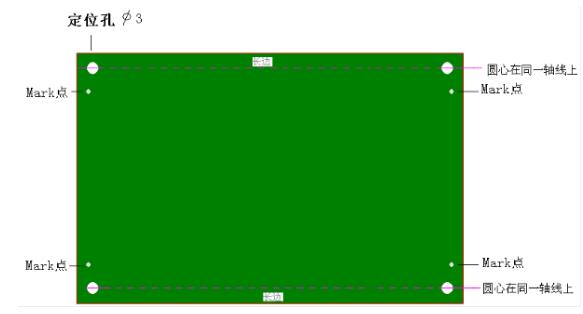
2.About Mark Points
Mark points should be labeled on the PCB board for the positioning of the SMD machine.
Specific location: in the diagonal corner of the board, can be round, or square pads, do not mix with other device pads. If there are devices on both sides, both sides should be labeled.
You can also consider adding MARK points on the collage.
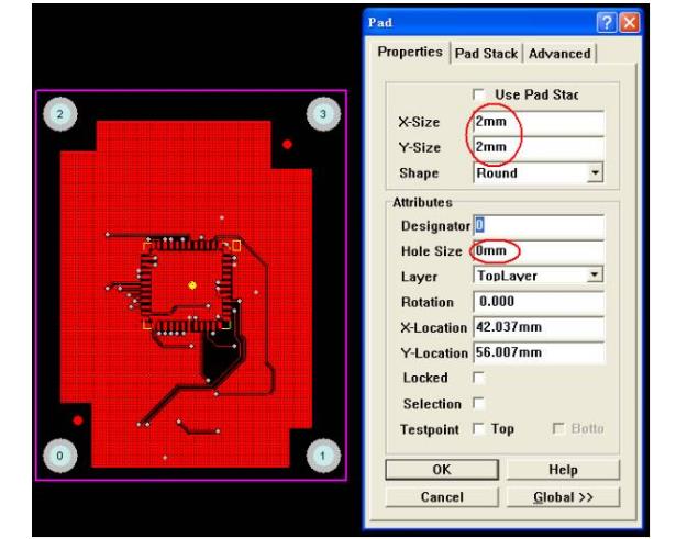
3.Design PCB, please pay attention to the following points:
a.The shape of the Mark points are symmetrical up and down or left and right.
b.The size of A is 2.0mm.
c.From the outer edge of the Mark point away from the range of 2.0mm, there should not be possible to cause misidentification of the shape and color changes. (Pad, solder paste)
d.The color of the Mark point should be different from the surrounding PCB color.
e.To ensure the accuracy of identification, the surface of the Mark point is plated with copper or tin to prevent reflection. For markers with only lines in their shape, light dots cannot be recognized.
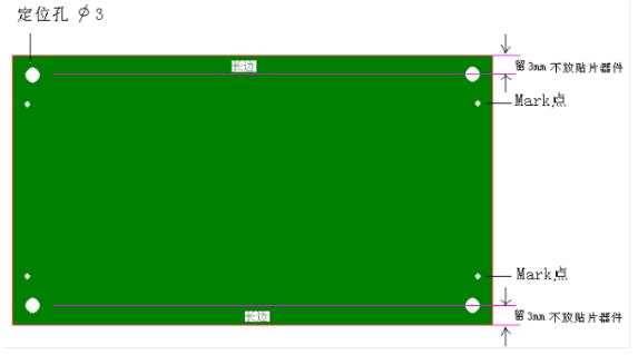
4.Whether to leave the edge of the board?
When drawing the PCB, leave a margin of not less than 3mm in the long side direction, which is used by the laminating machine to transport the board, and the laminating machine can't paste the device in this range. Don't put the device in this range.
For the boards with double-sided components, consider the problem of rubbing off the components and pads during the second reflow soldering.
It is recommended that the side with fewer wafers should not be placed within 5mm from the edge of the long side. If the board area is really limited, the art edge can be processed on the long side of the connecting board.
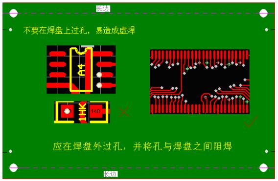
5.Do not directly on the pad through the hole
The soldering pad through the hole, the reflow soldering will have solder paste into the hole, resulting in the device pad lack of tin, resulting in virtual soldering, as shown in the following figure.
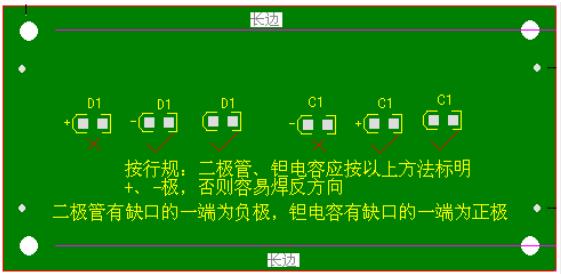
6.Polarity marking of diode and tantalum capacitor
The polarity marking of diode and tantalum capacitor is in accordance with the regulation, so as not to let the staff of PCBA factory solder in the wrong direction based on their experience. As shown in the picture:
7.About Silk Screen and Labeling
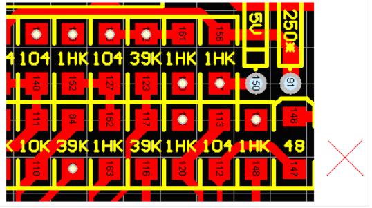
Please hide the device model number. This is especially true for boards with high device density. Otherwise, it will be confusing to find the soldering position.
Don't just mark the model number without labeling. As shown in the figure below, it will cause the programmer to be unable to program the SMD machine.
The font size of the silkscreen characters should not be too small, and the character placement should be staggered across the hole to avoid misreading.
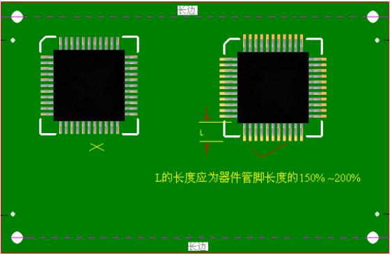
8.IC pads should be extended.
SOP, PLCC, QFP and other packaged IC, the length of the PCB soldering pad = IC foot length × 1.5 is appropriate, so that when soldering by hand with a soldering iron, the chip foot and PCB soldering pads, tin fused into one. As shown in the picture:
9.About the width of IC pads.
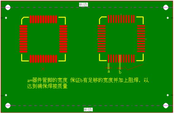
SOP, PLCC, QFP and other packages of IC, drawing PCB should pay attention to the width of the pad, PCB pad a width = IC foot width (datasheet in the Nom. value), do not recommend to widen, to ensure that the two pads between the distance between the b there is enough width, to avoid resulting in continuous welding. As shown in the figure:
10.Place the device do not rotate any angle
Because of the labeling machine can not rotate any angle, can only rotate 90 ℃, 180 ℃, 270 ℃, 360 ℃.
The following figure B rotated 1 ℃, after mounting the device pins and circuit board pads, the angle will be wrong 1 ℃, thus affecting the welding quality.
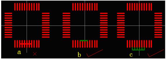
11.Neighboring pins should pay attention to the shorting problem
The following figure a shorting method, not conducive to worker identification, and welding is not aesthetically pleasing.
If the drawing according to Figure b, Figure c method of shorting and resistance welding, welding out of the effect is not the same.
As long as you make sure that each pin is not connected, the chip will have no short-circuit phenomenon, and the appearance is also beautiful.
12.About the middle pad under the wafer
For wafers with a belly, it is recommended to shrink the middle pad so that the distance between it and the surrounding pads is increased to minimize the chance of short-circuiting.
13.The thickness of the two devices should not be tightly lined up together
Higher thickness of the two devices so that the layout of the board will result in the second device paste paste machine touches the front of the device has been pasted, the machine will detect the danger, resulting in automatic power failure of the machine.
14.BGA packaging
Since BGA packaging is relatively special, its pads are under the chip, the outside can not see the welding effect.
In order to facilitate rework, it is recommended to play two Hole Size: 30mil positioning holes on the PCB board in order to locate the stencil during rework.
Warm tips: the size of the positioning holes should not be too large or too small, so that the needle is inserted into the needle does not fall, does not shake, inserted a little bit tighter as appropriate, otherwise the positioning is not allowed.
15.PCB board with what color?
It is not recommended to make it red. Red circuit boards in the red light source of the camera in the chip mounter is white, can not go into the travel design, not convenient for the chip mounter for soldering.
16.About the large devices under the small devices
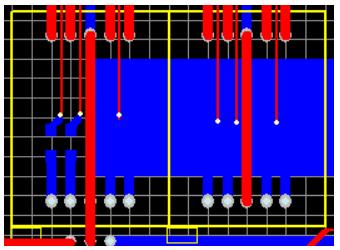
Some people like to arrange small devices in the same layer of large devices under, for example: digital tube under the resistor, as shown below:
Such a layout will cause difficulties for repair, repair must first remove the digital tube, may also cause damage to the digital tube. It is recommended to arrange the resistor under the digital tube to the Bottom side, as shown in the following figure:
17.The connection between the copper cladding and the soldering pad affects the melting of the solder.
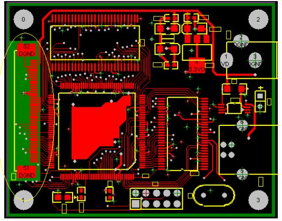
Since the copper cladding will absorb a lot of heat, it is difficult for the solder to melt sufficiently, thus forming a virtual solder. As shown in the figure:
Figure a, the device pads are directly connected to the copper cladding, Figure b, although the 50Pins connector is not directly connected to the copper cladding, but because the middle two layers of the four-layer board are large-area copper cladding, so Figure a, Figure b will be due to the copper cladding to absorb a large amount of heat, resulting in the paste can not be fully melted.
The body of the 50-pin connector in Fig. b is a plastic that is not resistant to high temperatures. If the temperature is set high, the body of the connector will melt or deform, and if the temperature is set low, the copper lamination absorbs a large amount of heat, resulting in the solder paste not being able to melt sufficiently. Therefore, it is recommended to isolate the pads from the large-area copper cladding.

Nowadays can use software to draw, design and layout PCB engineers more and more, the design is complete, and can be very good to improve the efficiency of welding, need to focus on the above elements. Cultivate good drawing habits, and can communicate well with the PCB and PCBA processing plant, is a PCB engineer to consider.