PCB Stamp Holes
In order to facilitate the separation of PCBs during PCB assembly, a small contact area is kept in the middle, and the holes in this area are called stamp holes. The reason for the name ‘stamp holes’ is that when the PCBs are separated, they are left with an edge like a stamp.
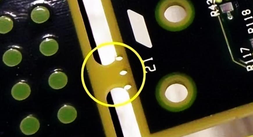
PCB Stamp Hole
PCB Vias VIA
In many cases, you will see mounting holes surrounded by tiny vias. There are 2 main types of mounting holes here: plated and unplated. There may be 2 reasons to use perforations around PCBs:
1.When we want to connect the hole to an inner layer (e.g. GND in a multi-layer PCB).
2.In the case of unplated holes, when we want to connect the upper and lower pads.
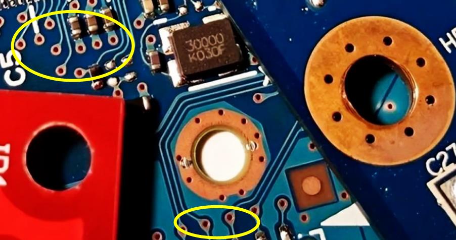
PCB Through Hole
Solder Resistant Solder Pads
One of the defects of wave soldering is that solder bridges tend to appear during the process of soldering SMDs. As a solution, it has been found that the use of extra pads at the end of the original pins can solve the problem. Extra pads are 2-3 times wider than normal pads.
It is also known as solder steal because it absorbs excess solder and prevents solder bridging.
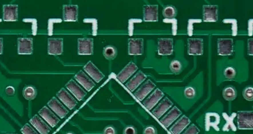
Solder Resistant Welding Pads
Baseline Marking (Mark Point Marking)
A bare copper circle within a larger bare circle. The datum mark is used as a reference point for the pick-and-place (PnP) machine. The datum mark is located in three places:
1.In the panel.
2.In addition to QFN, TQFP and other small pitch parts.
3.At the corners of the PCB.
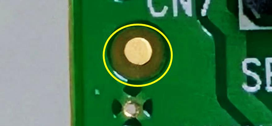
Mark point marking
Spark Gap
Spark gaps are used for ESD, electrical surge and overvoltage protection. High voltage can ionise the air between two terminals and create a spark between them before damaging the rest of the circuit. The use of this type of protection is not recommended, but it is better than nothing, the main disadvantage being that the effectiveness varies over time.
The breakdown voltage can be calculated by the following formula: V = ((3000 × p × d) + 1350)
Where ‘p’ is the atmospheric pressure, ‘d’ is organised in millimetres for the distance.
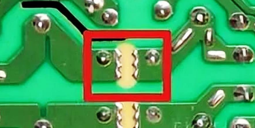
spark gap
PCB Conductive Button
If you've ever taken apart a remote control or an abacus, you'll have seen this mark. The conductor button consists of 2 staggered (but not connected) terminals. When the rubber button on the keyboard is pressed, the two terminals are connected because the bottom of the rubber button is electrically conductive.

PCB Conductive Keys
Fuse Alignment
Similar to a spark gap, this is another inexpensive technique for using PCBs. Fuse routing is the necking of power cables and is a disposable fuse. The same assembly can be used as a PCB jumper to remove specific connections by simply etching the necking trace (PCB jumpers can be found on the reset lines on some Arduino UNO boards).
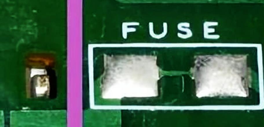
Fuse Alignment
PCB Slotting
If you look at the PCB of a high voltage device such as a power supply, you may notice that there are air pockets between some of the alignments.
Repeated temporary arcs in the PCB can cause the PCB to carbonise, leading to short circuits. In order to do this, you can add wiring slots in the suspected area, the area will still appear arc, but not carbonised.
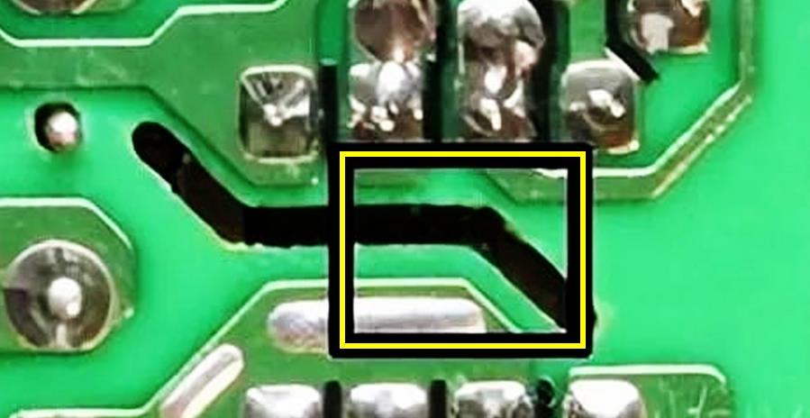
PCB Slot