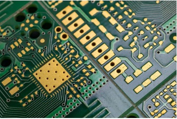
Electroless gold plating, commonly associated with surface finishes like ENIG (Electroless Nickel Immersion Gold) and ENEPIG (Electroless Nickel Electroless Palladium Immersion Gold), plays a critical role in modern PCB manufacturing. Unlike electroplating, this process does not require external current; instead, gold is deposited via a controlled chemical reaction. This method provides a uniform, highly reliable, and corrosion-resistant surface suitable for fine-pitch components, wire bonding, and RF circuits.
1. Working Principle of Electroless Gold Plating
Electroless gold plating is typically the final step in the ENIG or ENEPIG process. It involves a displacement reaction where gold is deposited onto a pre-plated nickel (Ni) or palladium (Pd) surface without using electricity. The key chemical reaction occurs in a heated solution containing potassium gold cyanide (KAu(CN)₂) and a reducing agent such as sodium hypophosphite. The gold is reduced and forms a thin, consistent layer on the catalytic metal surface.
The typical thickness of the electroless gold layer ranges from 0.03 to 0.05 μm, sufficient to prevent nickel oxidation and provide excellent solderability and wire-bonding characteristics.
2. Key Advantages in PCB Applications
Electroless gold plating offers several technical benefits in PCB applications:
Excellent Surface Planarity: Critical for fine-pitch components like BGA and QFN packages.
Superior Wire Bonding Compatibility: Gold is ideal for both gold and aluminum wire bonding, especially in ENEPIG.
Corrosion Resistance: The gold layer protects the underlying nickel from oxidation, ensuring long-term solderability.
Consistent Thickness: The autocatalytic nature of the reaction ensures uniform deposition, even on complex geometries.
Lead-Free and RoHS Compliant: A critical factor for modern environmental regulations.
These properties make electroless gold plating ideal for high-reliability sectors, including aerospace, telecommunications, medical electronics, and military applications.
3. Typical Surface Finish Systems Involving Electroless Gold
(1) ENIG (Electroless Nickel Immersion Gold)
Structure: Cu → Ni (3–6 μm) → Au (0.03–0.05 μm)
Widely used for general-purpose PCBs with BGA pads, exposed contacts, and controlled impedance applications.
(2) ENEPIG (Electroless Nickel Electroless Palladium Immersion Gold)
Structure: Cu → Ni (3–6 μm) → Pd (0.1–0.3 μm) → Au (0.03–0.05 μm)
Offers enhanced protection against nickel corrosion and is more suitable for aluminum wire bonding.

4. Process Control and Manufacturing Challenges
While electroless gold plating offers distinct advantages, it introduces several challenges:
Nickel Corrosion (“Black Pad” Defect): Improper control during the immersion gold step can lead to intermetallic corrosion of nickel, reducing solder joint reliability.
Bath Life Management: The gold plating bath has limited stability and must be tightly controlled for pH, temperature (typically 80–85°C), and chemical concentration to avoid defects.
Wastewater Treatment: Gold-containing wastewater is expensive to treat and highly regulated. Efficient recovery systems are required.
Compatibility with Solder Paste: Inconsistent gold thickness or contamination can affect solderability and wetting behavior during reflow soldering.
To ensure high yield and performance, PCB manufacturers must maintain strict quality control, including bath analytics, surface roughness measurement, and adhesion testing.
5. Future Trends and Alternatives
With increasing demand for high-frequency and miniaturized devices, electroless gold plating continues to evolve. Some emerging trends include:
Selective ENEPIG: Applying ENEPIG only on specific RF pads to reduce cost.
ENIG for HDI boards: Optimized for fine lines and microvias.
Green chemistry solutions: Developing cyanide-free or low-cyanide gold baths to meet environmental goals.
Conclusion
Electroless gold plating is a cornerstone surface finish in high-reliability PCB fabrication, offering precise, uniform deposition and excellent performance for advanced applications. However, its success depends heavily on process stability and materials compatibility. As electronics continue to shrink and accelerate, the demand for robust surface finishes like ENIG and ENEPIG will only grow, pushing the boundaries of plating technology further.