In the modern PCB circuit board manufacturing process, ENIG and gold plated are two common surface treatment methods. With the increasing speed of IC processing, the IC pin pitch is getting smaller and smaller, and the traditional vertical tin spraying process is difficult to form a flat solder layer, which brings challenges to the SMT placement process. In addition, the storage life of tin-sprayed boards is short, and the gold plated process can exactly solve these problems. Therefore, gold plated pcb board is widely used in high-density and miniaturized surface mount process.
During the R&D phase, PCBs often need to be stored for weeks or even longer before being put into use due to the long procurement cycle of components. Compared to tin boards, gold plated pcb boards have a longer storage life, making them the preferred choice for many engineers. In addition, at the prototype stage, the cost of the gold plating process is not much different from that of lead-tin alloy boards, further increasing its application value.
What is gold plated pcb board?
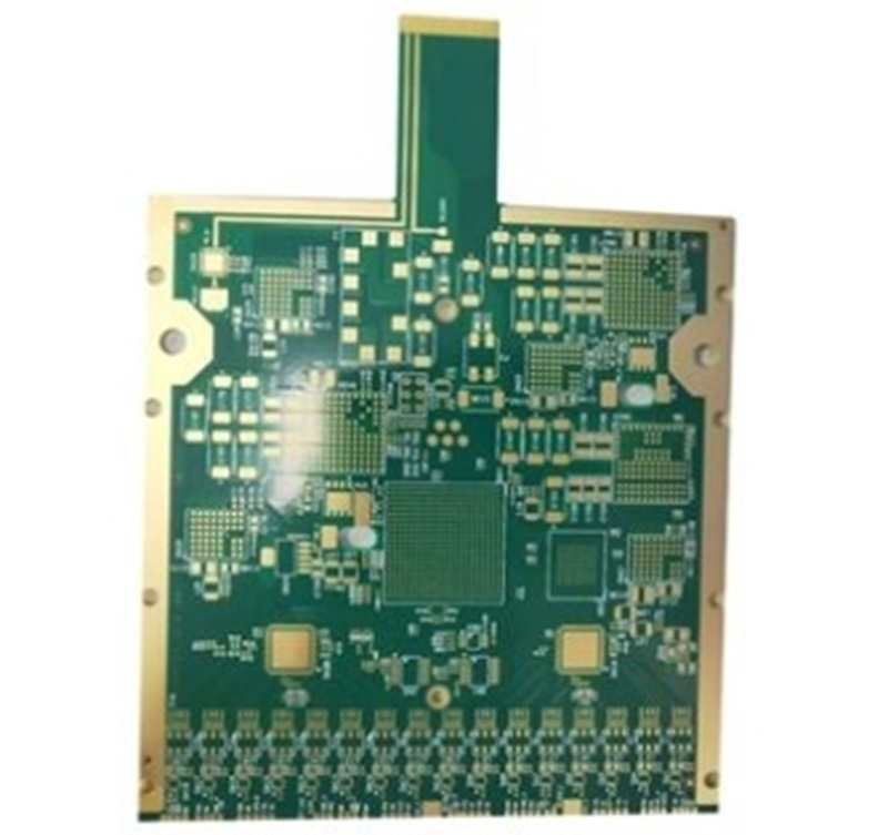
Gold plated, also known as electrolytic gold and electro-nickel-gold boards, is a method of forming a nickel-gold coating on the surface of a PCB through an gold plated process. The basic principle is to dissolve nickel and gold (usually gold salts) in a specific chemical solution. After the PCB is energized in the plating tank, the metal ions are deposited on the surface of the copper foil to form a coating. Gold plated is divided into soft gold and hard gold (such as gold finger special hard gold). Gold plated pcb board has the advantages of high hardness, abrasion resistance, not easy to oxidize, etc., and is widely used in electronic equipment.

gold plated pcb board
What is ENIG?
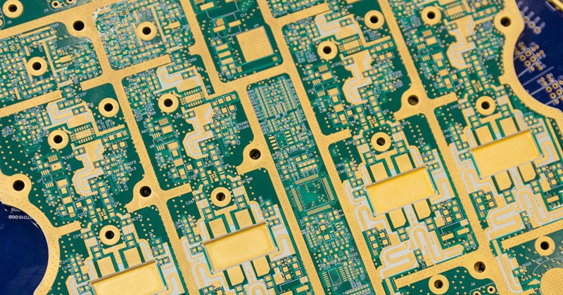
ENIG is a chemical redox reaction to form a metal plating layer, which usually results in a thicker layer of gold plating, and is therefore also known as immersion gold. The process deposits a uniform, dense layer of nickel-gold alloy on the copper surface of the PCB by chemical deposition, providing good solderability and oxidation resistance.

ENIG pcb board
The main difference between ENIG and gold plated
1. Thickness and Color of Metal Plating
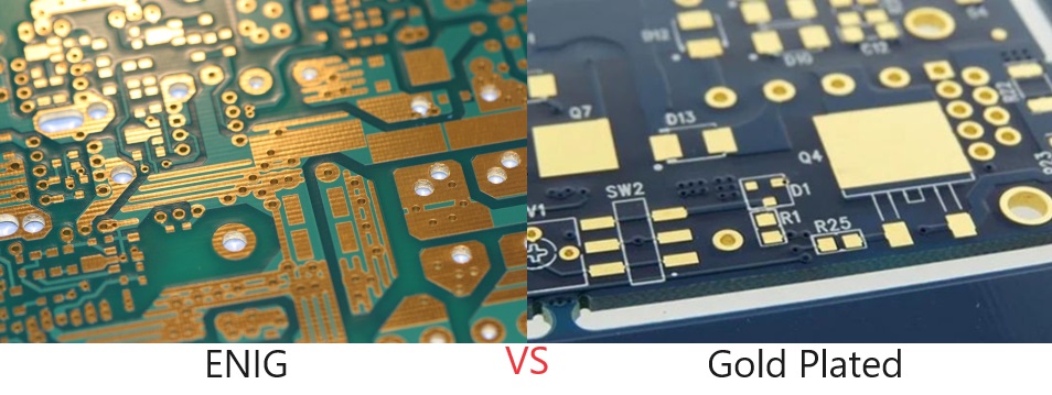
The thickness of the gold layer formed by the ENIG process is thicker than that of gold plated, and the color of the ENIG boards usually shows a more obvious golden color, which makes the visual effect more preferred by customers compared to gold plated.
2. Welding Performance
The welding performance of ENIG process is better than gold plated, and welding defects are less likely to occur during the welding process, thus reducing customer complaints. In addition, the internal stress of ENIG is easier to control, which is more friendly to products that require binding process. Gold plated pcb board, on the other hand, is not suitable as a gold finger material for conductive silver adhesive due to its relative hardness.
3. Signal Transmission Characteristics
Since the ENIG process only covers the nickel-gold layer in the soldering area, it does not affect the conductivity of the copper layer of the PCB, which ensures the stability of signal transmission.

ENIG VS Gold Plated
4. Oxidation resistance
The ENIG PCB has a denser molecular structure and is less prone to oxidation, providing better long-term storage performance than gold plated pcb board.
5. Suitable for high density designs
With the PCB design tends to high-density, line width and pitch has been reduced to 3-4 MIL. electroplating is easy to lead to short-circuit, while the gold deposition process only in the pad area of the deposited nickel-gold layer, can effectively avoid short-circuit problems.
6. Soldermask bonding
PCB with ENIG process, the solder resist layer and the copper layer of the bonding force is stronger, engineering compensation design is not easy to affect the line spacing.
7. Application
In general, for PCBs with high requirements for flatness, the ENIG process is usually chosen. In addition, the ENIG board in the subsequent assembly process is not easy to appear "black pad" phenomenon, to ensure long-term reliability.
ENIG and gold plated pcb boards have their own advantages, in the actual application of the need to choose according to the specific needs of the product. If the PCB needs longer storage life, better soldering performance and oxidation resistance, ENIG PCB is a more ideal choice; for applications requiring high wear resistance, such as gold fingers, gold plated pcb board still has the advantage.