A Trustworthy PCB and Electronic Manufacturing Enterprise! Contact Us


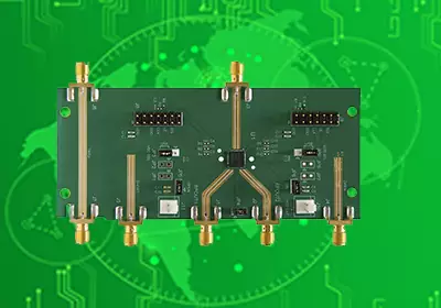
Flying probe test, also known as flying probe technology, is an automated process designed to check the electrical connectivity and performance of PCBs. This method employs specialised equipment, known as flying probe testers, which feature multiple removable probes that establish contact with the PCB's circuitry to measure various electrical parameters.
Within the electronics manufacturing industry, flying probe test technology is a common means of circuit board testing. The advantage is that the connection performance between interfaces can be evaluated without direct physical contact, thus ensuring efficient and accurate testing. In addition, flying probe testing can reveal defects that are difficult to capture with other test techniques, such as deviations in the position of through-holes on the board, spatial layout errors, motor connector pin offsets, and chip pin displacements.
What is the difference between pin testing and test stands? What are the advantages of each?
Flying probe test: Flying probe test is the use of 4 to 8 probes on the circuit board for high-voltage insulation and low-resistance conductivity test, test line open and short circuit, do not need to make special test fixtures. Flying probe test is directly to the PCB board mounted on the flying probe test machine, and then run the test programme can be tested.
The advantage of flying probe test is that its test method and operation process is extremely convenient, saving the cost of testing, eliminating the time to make test racks, improve the efficiency of shipping, suitable for PCB small batch production.
The test fixture, is for mass production of PCB boards for on-off test and make a special test fixture, the production cost is higher, but the test efficiency is better, the return order is not charged. In the test technology for the purpose, flying probe test is currently suitable for use in small quantities and samples of electrical test equipment, but if you want to use in large quantities in production, due to the slow speed of measurement and expensive equipment will make the test cost significantly higher, while the general-purpose and specialised type of PCB boards used for whatever level, as long as the production volume reaches a certain number of test costs can be achieved to achieve economies of scale. Standard, and only about 2 ~ 4% of the selling price, which is why the general-purpose type and special-purpose type for the current mass-production type of test machine types of the main reasons.
The working principle of flying probe inspection technology is based on the combination of a series of high-precision electromagnetically driven mechanical assemblies with circuit inspection equipment, which follows a predefined test programme and thoroughly scans the circuit board for all circuit nodes to be tested. During the inspection process, the flying probe head establishes an electrical connection to the test points, which is followed by precise measurements of the electrical parameters by the inspection instrument. These measurements are analysed by the processor to produce test results. These results are presented in a variety of ways and can be saved and processed by the tester or by an automated system.

Capabilities of flying probe test technology
Flying probe testingis not only good at detecting shorts and opens, but by equipping it with special actuators it is also able to cope with more complex parametric tests. The advanced probe design allows for simultaneous probing and testing of both sides of a multilayer board, significantly reducing the time required to test each side individually. In addition, the flying probe test system has a variety of architectures for different test requirements, including:
Signal Integrity Assessment: Using TDR (Time Domain Reflectance) technology or associated probes and dedicated instrumentation, flying probe test can analyse a wide range of characteristics of high-speed, high-frequency PCB alignments. These devices capture and measure signals in both the time and frequency domains to reveal potential defects in the signal path.
Phase Difference Analysis: Using specially designed probes that send high-frequency signals between the reference path and the signal path, flying probe testing is able to measure the phase difference between the two. This test method eliminates the need for additional isolation tests to effectively assess crosstalk between PCB alignments.
High Voltage Insulation Test: Conventional resistance tests may not be able to accurately identify possible isolation defects in a PCB. Although the insulation resistance between two alignments may be sufficient to pass conventional tests, it may still be below specification. For this reason, flying probe testing employs high voltage stress testing, combining a high voltage generator, specialised flying probes and a high resistance meter to ensure accurate assessment of insulation performance.
Micro-short circuit detection: Tiny conductive strips may cause micro-shorts on the PCB. These strips may burn out during high-voltage stress testing, leaving a carbonised residue that creates a high-resistance conductive path. Flying probe testing accurately identifies micro-short problems by applying a low voltage through the micro-short detection probe and gradually increasing it to the test voltage to check the resistance between two alignments on the PCB.
Kelvin DC Precision Measurement: For close-pitch PCB patterns such as BGAs, Kelvin DC measurement technology provides extremely high measurement accuracy. The technique requires flying probes equipped with force and sensing pins, and compensates for losses in the test probes through the Kelvin connection, ensuring accurate measurement results.
The impact and effect of flying probe test on PCBA is mainly reflected in the following aspects:
Improve product quality and yield: Flying probe test can accurately detect PCBA short circuit, open circuit and other problems through high-voltage insulation and low-resistance conductivity test to ensure that the electrical performance of PCBA meets the standard, thus significantly improving the yield of the product.
Suitable for small batch production and sample test: Flying probe test is especially suitable for small batch production and sample test of PCBA. It is easy to operate, no need for special test fixtures, directly load the PCBA into the flying probe tester can be tested, saving the test cost and improving the shipping efficiency.
Improve test efficiency and accuracy: Flying probe test adopts multiple motor-driven probes, which can move quickly and make precise contact with device pins for efficient electrical performance measurement. Its high testing accuracy enables it to detect tiny defects, such as components with 0.1mm pitch.
Save time and cost: Flying probe testing eliminates the need to make special test fixtures, reducing the time and cost of making test stands. Especially in small batch production, the efficiency and cost advantages of flying probe testing are more obvious.
Suitable for a variety of application scenarios: Flying probe test is not only suitable for the initial quality check of PCBA, but also can monitor the quality of components after reliability stress test. In automotive electronics and other fields that require high reliability, flying probe test can provide numerical comparisons before and after the experiment, reduce human measurement errors and improve the quality of the experiment.
The size and configuration of flying probe test systems vary depending on the number of connectors. For example, some systems may be equipped with as many as 16 header connectors, eight on the top of the PCB and eight on the bottom. Of course, the cost of the system increases in proportion to the number of connectors.
Flying probe test technology is an important part of circuit board inspection in the electronics manufacturing industry due to its efficiency, accuracy and flexibility. Whether it is for small quantities or prototypes, flying probe testing offers a reliable solution. Despite the challenges of mass production, its unique advantages make it an indispensable test tool that continues to drive the electronics manufacturing industry.