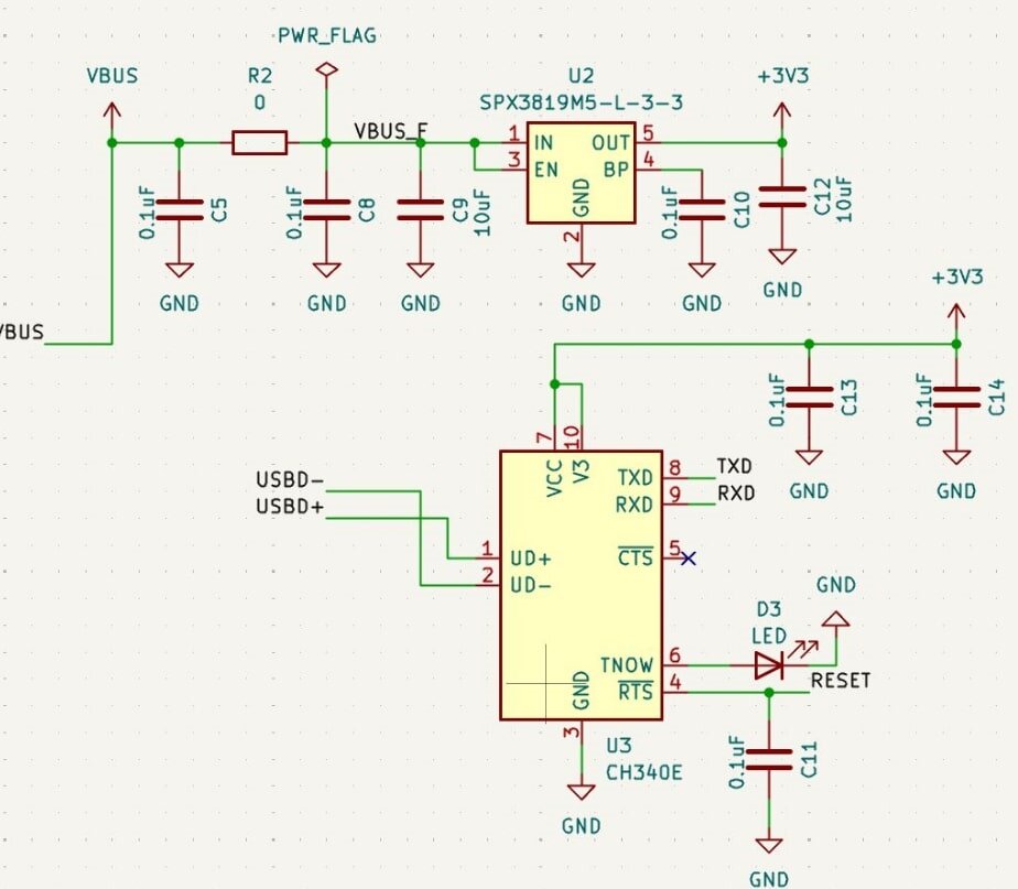
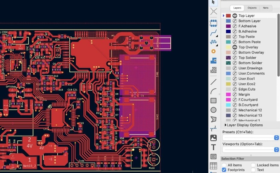
PCB board schematic design is crucial for manufacturing reliable circuit boards. A PCB board schematic is an electrical connection diagram drawn by an electronic engineer based on design requirements. It uses standardized electronic component symbols to describe how each component in the circuit interacts to achieve the intended function. For example, in a power module schematic, you can see the input voltage being rectified, regulated, filtered, and then outputting a stable DC voltage. Although a schematic may appear to be just a combination of lines and symbols, to an engineer, it represents the flow of current, the path of signals, and the logical structure of the entire system.

pcb board schematic
Common components in PCB board schematic design:
1. PCB board schematic symbols
Before delving into schematics, familiarize yourself with common symbols:
Resistors: Zigzag lines or rectangles.
Capacitors: Two parallel lines (polarized capacitors include positive and negative markings).
Diodes: Triangles pointing towards the lines, indicating polarity.
Integrated Circuits (ICs): Rectangles with marked pins.
Ground and Power Symbols: "GND" indicates ground, "Vcc" indicates power.
2. Tracing Nets (Connections/Wires)
Nets are the lines that connect components. Each net may have a label, such as "Vcc" or "GND," to identify its function. Using these labels helps understand how power and signals flow in the circuit.
3. Component Values and Labels
Each component has a designation (e.g., R1 represents a resistor, C1 represents a capacitor) and a value (e.g., 10kΩ represents a resistor, 100µF represents a capacitor). These details are crucial for identifying components and their role in the circuit.
Drawing the schematic drawing is the most critical stage and typically includes the following steps:
1. Placing Key Components
Place core chips, power modules, interface devices, etc., on the canvas according to their functional modules.
2. Connecting Signal and Power Lines
Connect component pins using nets.
Net labels can be used to identify signals names, reduce crosshairs, and improve readability.
3. Add auxiliary circuits such as power supply, ground, and decoupling capacitors. For example:
Add a decoupling capacitor (0.1µF) next to each IC power supply pin.
Analog and digital grounding.
Power supply filtering and protection circuit design.
4. Naming and Labeling
Add clear names and annotations (e.g., VCC_3V3, UART_TX, R101, etc.) to each signal, device, and interface for easy reading and later debugging.
5.Hierarchical Design
For complex circuits (such as main control + power supply + communication + sensing modules), a hierarchical structure is recommended. Each functional module should be on a separate page, and the main page should provide unified access.

pcb board schematic
PCB Design to Production
To understand the importance of PCB board schematics, we need to understand the entire PCB design and manufacturing process. Typically, a PCB project, from concept to finished product, can be divided into the following stages:
1. Requirements analysis and circuit design
2. Drawing PCB board schematics
3. Generating netlists and importing them into the PCB design
4. PCB layout and routing
5. Design rule checking (DRC) and file output
6. PCB fabrication
7. SMT assembly and soldering
8. Testing and verification
PCB board schematic design is both a technical and logical task. It requires designers to understand circuit principles, possess systematic thinking, a strong sense of standards, and a rigorous attitude. Designing a high-quality PCB board schematic is one of the most critical steps in the entire hardware development process. It not only determines whether the circuit functions correctly but also affects subsequent PCB layout and routing, debugging, and mass production efficiency. Mastering PCB board schematic design specifications can reduce project risks and improve product reliability and R&D efficiency.