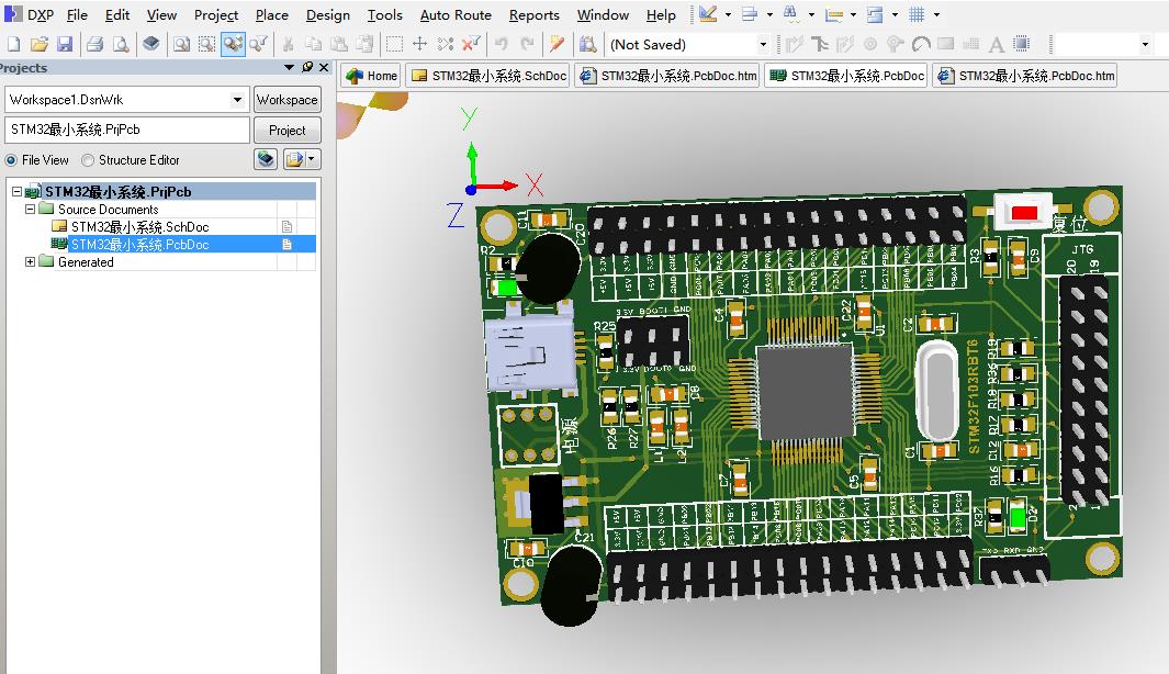
The layout of the components and the routing of the wires are very important in order to obtain the best performance from an electronic circuit. In order to PCB design quality, low cost PCB, should follow the following general PCB design principles:
1.PCB layout
First, consider the size of the PCB size. PCB size is too large, the printed line is long, impedance new, anti-noise ability to decline, the cost is also new. Too small, the heat dissipation is not good, and the neighbouring lines are susceptible to interference. After determining the size of the PCB, determine the location of special components. Finally, all the components of the circuit are laid out according to the functional units of the circuit.
Observe the following PCB design principles when determining the location of special components:
(1) Try to shorten the connection between high-frequency components as much as possible, and try to reduce their distribution parameters and the electromagnetic interference between them. Components susceptible to interference should not be too close to each other, and input and output components should be as far away as possible.
(2) Certain components or wires may have a high potential difference between them, and the distance between them should be increased to avoid accidental short-circuiting due to discharge. Components with high voltages should be placed as far away as possible from hand reach during commissioning.
(3) Components weighing more than 15g should be fixed with brackets and then soldered. Components that are large and heavy and generate a lot of heat should not be mounted on the PCB, but on the bottom plate of the machine's chassis, and heat dissipation should be considered. Thermal components should be kept away from heat generating components.
(4) The layout of adjustable components such as potentiometers, adjustable inductor coils, variable capacitors, micro switches, etc. should take into account the structural requirements of the machine. If it is adjusted inside the machine, it should be placed on the PCB where it is convenient to adjust. If it is adjusted outside the machine, its position should be appropriate with the position of the adjusting knob on the main chassis panel.
(5) The location of PCB positioning holes and fixing brackets should be left.
According to the functional unit of the circuit. When laying out all components of the circuit, comply with the following PCB design principles:
(1) Arrange the position of each functional circuit unit in accordance with the flow of the circuit so that the layout facilitates the flow of signals and keeps the signals in the same direction as far as possible.
(2) Take the core component of each functional circuit as the centre and layout around it. Components should be arranged evenly, neatly, and compactly on the PCB.Minimise and shorten the lead wires and connections between components.
(3) For circuits operating at high frequencies, consider the distribution parameters between components. In general, components should be arranged in parallel as much as possible. In this way, it is not only aesthetically pleasing, but also easy to mount and solder, which makes it easy for mass production.
(4) Components located at the edge of the circuit board should not be less than 2mm away from the edge of the board. The best shape for the circuit board is rectangular. The length and width should be 3:2 or 4:3. When the size of the circuit board is larger than 200 × 150 mm, the mechanical strength of the PCB should be considered.

PCB Design
2.PCB Layout
The PCB design principles for wiring are as follows:
(1) The wires used for input and output should be avoided to be parallel to each other as much as possible. It is best to add the ground between the lines to avoid the occurrence of reverberation coupling.
(2) The minimum width of PCB lead wires is mainly determined by the adhesion strength between the lead wires and the insulated substrate and the current value flowing through them. When the thickness of copper foil for 0, 5mm, width of 1 ~ 15mm, through the 2A current, the temperature will not be higher than 3 ℃. Therefore, a lead wire width of 1.5mm is sufficient. For integrated circuits, especially digital circuits, a lead width of 0.02 to 0.3mm is usually chosen. Of course, as long as it is possible, it is better to use wide wires, especially for power and earth wires. The minimum lead spacing is determined by the worst-case insulation resistance and breakdown voltage. For integrated circuits, especially digital circuits, as long as the process allows, so that the pitch is less than 5 to 8 mil.
(3) PCB lead corners are generally rounded, and right angles or corners in high-frequency circuits will affect the electrical performance. In addition, try to avoid the use of large-area copper foil, otherwise, when subjected to heat for a long time, the copper foil is prone to expansion and peeling phenomenon. If a large area of copper foil must be used, it is best to use a grid. This is conducive to the elimination of volatile gases generated by heat between the copper foil and the substrate adhesive.
3.PCB pad design principles
PCB pad centre hole should be slightly larger than the device lead diameter. Pad is too large and easy to form a virtual welding. Pad outer diameter D is generally not less than (d + 1, 2) mm, where d is the lead aperture. For high-density digital circuits, the minimum diameter of the pad can be (d + 1, 0) mm.