Semiconductor materials are electronic materials with semiconductor properties (conductivity between conductors and insulators, resistivity in the range of 1mΩ-cm to 1GΩ-cm) that can be used to make semiconductor devices and integrated circuits. Elemental semiconductors refer to semiconductors formed by a single element such as silicon and germanium, while compounds refer to semiconductors formed by compounds such as gallium arsenide and phosphorous alumina. With the development of wireless communication, the application of high-frequency circuits is becoming more and more extensive. Today, we would like to introduce the semiconductor materials and processes suitable for RF circuits, microwave and other high-frequency circuits.
Gallium Arsenide GaAs
Gallium Arsenide (GaAs) has an electron mobility rate 5.7 times higher than that of silicon, making it very suitable for high-frequency circuits. The electrical characteristics of GaAs components in high frequency, high power, high efficiency, and low noise index are much better than silicon components. Spare-type GaAs field-effect transistors (MESFETs) or high electron mobility transistors (HEMTs/PHEMTs) can have a power added efficiency (PAE) of 80% at 3 V, which makes them very suitable for use in high frequency circuits.It is very suitable for high tier wireless communication with long distance and long communication time.
Gallium Arsenide (GaAs) components have a much higher electron mobility than silicon, so they are made using a special process.In the early days,they were MESFET metal semiconductor field effect transistors, which later evolved into HEMTs (high-speed electron mobility transistors), pHEMTs (high electron mobility transistors), and now HBTs (heterojunction two-carrier transistors).Hetero-Bipolar Transistors (HBTs) are GaAs components that do not require a negative power supply.Their power density, current drive capability,and linearity exceed those of FETs, making HBTs the optimal component choice for designing microwave amplifiers with high power, high efficiency, and high linearity. HBT is the best choice of component.HBT components have advantages in phase noise, high gm, high power density, collapse voltage and linearity. In addition, it can be operated with a single power supply, which simplifies the circuit design and the difficulty of sub-system realization,and is very suitable for the research and development of RF and IF transceiver modules, especially microwave signal sources and high linearity amplifiers and other circuits.

Gallium arsenide production is very different from traditional silicon wafer production.Gallium arsenide needs to be manufactured using epitaxial technology,which is usually 4-6 inches in diameter,much smaller than the 12 inches of silicon wafers. Epitaxial wafers require special machines, and the cost of gallium arsenide raw materials is much higher than that of silicon,which ultimately leads to a higher cost for the finished gallium arsenide IC.There are two types of epitaxial wafers, one is chemical MOCVD and the other is physical MBE.
Gallium Nitride GaN
In broadband semiconductor materials, the development of Gallium Nitride (GaN) has been relatively slow due to the lack of suitable single crystal substrate materials, bit error density and other problems.However, after entering the 90s, with the continuous development of material growth and device technology level, GaN semiconductor materials and devices have developed very rapidly, and has now become a dazzling new star in broadband semiconductor materials.
GaN semiconductor materials application is the first in the field of light-emitting devices to achieve a major breakthrough. 1991,Japan's Nichia (Nichia) company first research and development of successful sapphire as a substrate for the GaN blue light-emitting diode (LED), and then realize the commercialization of the GaN-based blue and green LEDs. Utilizing GaN-based blue LEDs and phosphorescent technology,the company developed white light emitting device products featuring high life and low energy consumption. In addition, the company was the first to develop GaN-based blue semiconductor lasers.
GaN-based high-efficiency blue-green LEDs can be used to create large-screen full-color displays for indoor and outdoor dynamic information displays in a variety of applications. High efficiency white light emitting diode as a new type of energy efficient solid light source,the service life of more than 100,000 hours, can be compared with incandescent lamps to save 5 to 10 times the electricity,to achieve the dual purpose of saving resources and reducing environmental pollution. Currently,GaN-based LEDs are widely used, you may see it every day, in traffic signals, color video signage, children's toys, and even flash lamps.The success of GaN-based LEDs has led to a revolution in the optoelectronics industry.GaN-based blue semiconductor lasers are mainly used in the production of next-generation DVDs, which can increase the storage density of more than 20 times than that of the current CD-ROMs.
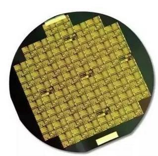
The use of GaN materials, but also to prepare ultraviolet (UV) light detector, which has a wide range of applications in flame sensing, ozone detection, laser detector. In addition, in terms of electronic devices, the use of GaN materials, can produce high-frequency, high-power electronic devices, is expected to play an important role in aerospace, high temperature radiation environment, radar and communications. For example, in the field of aviation aerospace, high-performance military flight equipment needs to be able to work at high temperatures, sensors, electronic control systems and power electronic devices, etc., in order to improve the reliability of flight, GaN-based electronic devices will play an important role, in addition to its high-temperature work without the need for refrigeration and greatly simplify the electronic system to reduce the weight of the flight.
Phosphor InP
InP is an important Ⅲ-V compound semiconductor material after silicon and GaAs.Almost at the same time as the development and research of the first-generation elemental semiconductor materials such as germanium and silicon, scientists have begun a lot of exploration of compound semiconductor materials.
As a new type of semi-insulated wafers, the emergence of InP (InP) is of great significance to improve and enhance the performance of InP-based microelectronic devices. The semi-insulated wafers prepared by high-temperature annealing process not only maintain the high-resistance characteristics of the traditional native doped iron substrate,but also greatly reduce the iron concentration, and significantly improve the electrical properties, uniformity and consistency. Currently, the quality of semi-insulated InP substrates needs to be improved.
Native semi-insulated InP is prepared by doping iron atoms during the single crystal growth process.In order to achieve the purpose of semi-insulation, the doping concentration of Fe atoms is relatively high, and the high concentration of Fe is likely to diffuse with the epitaxial and device processes. Moreover, due to the small coefficient of Fe condensation in phosphor,the InP single crystal ingot shows a clear doping gradient along the growth axis, with the Fe concentration at the top and bottom differing by more than an order of magnitude, making it difficult to ensure the consistency and uniformity of the single wafers cut from it.As far as the cut single InP wafers are concerned, due to the influence of the solid-liquid interface during growth, the Fe atoms are distributed in concentric circles from the center of the wafer outward,which obviously cannot meet the needs of some device applications. All these factors are the biggest obstacles to the quality of semi-insulated phosphor monolithic wafers.
In recent years, domestic and foreign studies have shown that the semi-insulating backing obtained by annealing low-resistance, non-doped InP wafers at high temperatures in a certain atmosphere can overcome the above problems. In the InP crystal, the formation mechanism of semi-insulation can be roughly summarized as two aspects: one is through the doping of a large number of the main (elements) to compensate for the shallow sizing to achieve a semi-insulated state, the primary doped semi-insulated plutonium phosphide belongs to this kind of situation; the other is through the formation of new defects to make the shallow sizing of the concentration of the main reduction, while the resident large number of the main (elements) also occurred to compensate for the non-doped semi-insulated plutonium phosphide belongs to this kind of category, the new defects can be formed at high temperature annealing, and the new defects can be removed in a high-temperature annealing treatment, so as to overcome the above problem. New defects can be formed in the process of high-temperature annealing and irradiation. According to this idea, the Chinese Academy of Sciences Institute of semiconductor researchers have taken three steps to prepare non-doped semi-insulated phosphor phosphide backing: first of all, the liquid-sealed straight pulling method to pull the production of high-purity, low-resistance non-doped phosphor phosphide monocrystals (the surface of the low-resistance), and then cut it into a certain thickness of the wafer and encapsulation of quartz tubes, and finally in the right atmosphere under the conditions of high-temperature annealing treatment. The researchers conducted dozens of comparative annealing experiments in pure phosphorus atmosphere and iron phosphide atmosphere. After comparative testing and analysis, it was found that the semi-insulated phosphor wafers annealed in Fe-phosphide atmosphere not only had fewer defects,but also had good uniformity.
In order to further investigate the practical effect of this annealed substrate on the neighboring epitaxial layers,the researchers used the molecular Cambodian epitaxy technique to grow identical InAlAs epitaxial layers on natively doped and semi-insulated phosphor substrates annealed in Fe-phosphide atmosphere, respectively. The test results show that the latter is more favorable for growing epitaxial layers with good crystalline quality. In addition, after injecting the same dose of Si ions into these two substrates and after fast annealing, the Hall test results confirm that the latter can improve the start-up efficiency of the injected ions more significantly.
Phosphorite wafers are commonly used in the manufacture of high-frequency, high-speed, high-power microwave devices and circuits, as well as satellites and solar cells for outer space. It is the preferred backing material in the rapidly developing field of fiber optic communications. In addition, InP-based devices have advantages in IC and switching applications. The successful development of this new type of semi-insulated phosphor wafer will play an important role in the field of national defense and high-speed communications. The 13th Research Institute of China Electronics Technology Group (CETG) has successfully fabricated high electron mobility transistors with an operating frequency of 100 GHz using this new type of semi-insulated phosphine pure phosphorus substrate.
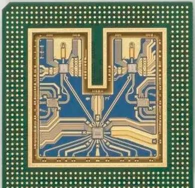
SiGe
In the 1980s, IBM added Ge to improve Si materials in order to increase the speed of electron flow, reduce power consumption and improve functionality, but it accidentally succeeded in combining Si and Ge. Since IBM announced that SiGe had entered mass production in 1998, SiGe has become one of the most valued wireless communication IC process technologies in the past two to three years.
According to the material characteristics, SiGe has good high-frequency characteristics, good material safety, good thermal conductivity, and process maturity, high degree of integration, and has the advantage of lower cost. In other words, SiGe can not only directly utilize the existing 200mm wafer process of semiconductors to achieve a high degree of integration, which creates economic scale, but also has high-speed characteristics comparable to GaAs. With the recent investment of IDM factories, SiGe technology has been gradually in the cut-off frequency (fT) and the breakdown voltage (Breakdown voltage) is too low to improve the problem and become increasingly practical.
Currently, this process technology developed by IBM has integrated high-efficiency SiGe HBT (Heterojunction Bipolar Transistor) 3.3V and 0.5μm CMOS technology, which can be utilized for analog, RF, and mixed-signal configurations using active or passive components.
SiGe offers the integration, yield, and cost advantages of silicon with the speed benefits of Class 3 to 5 semiconductors such as GaAs and InP. SiGe semiconductor technology can be used to integrate high-quality passive components by adding metal and dielectric stacks to reduce parasitic capacitance and inductance. In addition, device behavioral changes with temperature can be designed by controlling the alumina doping. the SiGe BiCMOS process technology is compatible with virtually all of the new technologies in the silicon semiconductor Very Large Synthesis Circuit (VLSI) industry, including Silicon on Insulator (SOI) technology and trench isolation technology.
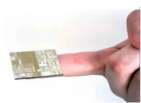
However, in order to replace GaAs, silicon needs to continue to work on breakdown voltage, cutoff frequency, and power consumption.
RF CMOS
RF CMOS processes can be categorized into two main types: the bulk silicon process and the silicon on insulator (SOI) process. Because of the diode effect between the source and drain to the substrate of the physical silicon CMOS, resulting in a variety of disadvantages, most experts believe that it is impossible to use this process to produce high power and high linearity switch. Unlike silicon, RF switches made using the SOI process can connect multiple FETs in series to cope with high voltages, just like GAAS switches.
Although the pure silicon CMOS process was considered to be suitable only for designs with more digital functions and not for RF IC designs with analog circuits, after more than a decade of hard work, with the improvement of CMOS performance, the cooperation of foundries with process technologies below 0.25mm, and the trend of integration of wireless communication chips, the RF CMOS process has not only become a hot topic of academic research, but has also aroused the interest of academics in the field. The RF CMOS process is not only a hot topic in academic research, but has also attracted the attention of the industry. The biggest advantage of adopting RF CMOS process is of course the high degree of integration of RF, baseband and memory components into one, and at the same time reduce the cost of components. However, the crux of the matter still lies in whether RF CMOS can solve the problems of high noise, low insulation and Q value, and reduce the increased process cost to improve performance in order to meet the stringent requirements of RF circuits for wireless communications.
Currently, most of the products that have adopted RF CMOS for RF ICs are Bluetooth and WLAN RF ICs, which have more relaxed RF specifications. For example, Bluetooth chip makers such as CSR, Oki, Broadcom, etc. have already launched Bluetooth transmitters using CMOS; Intel Corporation announced that it has already developed Bluetooth transmitters that can support all the current Wi-Fi standards (Wi-Fi, Wi-Fi, Wi-Fi, etc.). Intel Corporation announced that it has developed a prototype of an all-CMOS process direct-conversion dual-band wireless transceiver that supports all current Wi-Fi standards (802.11a, b, and g) and complies with the expected requirements of 802.11n. The prototype includes a 5GHz PA and easily separates transmitter and receiver functions. WLAN chip vendors such as Atheros and Envara have also recently introduced fully CMOS processed multimode WLAN (.11b/g/a) RF chipsets.
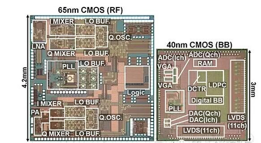
The specifications of cell phone RF ICs are very strict, but the ice has been broken. Silicon Labs was the first to use digital technology to enhance the low-intermediate frequency (LIF) to baseband filters and digital channel selection filters, in order to reduce the problem of CMOS noise is too high in the production of the Aero LIF GSM/GPRS chipset, Infineon immediately followed suit, and also a large number of RF CMOS process products, and Qualcomm, after the acquisition of Berkana, also vigorously adopt RF CMOS process, a group of new RF manufacturers without exception have adopted RF CMOS process, even the most advanced 65-nanometer RF CMOS process. After Qualcomm acquired Berkana, it also vigorously adopted the RF CMOS process. A number of new RF manufacturers have adopted the RF CMOS process without exception, even the most advanced 65nm RF CMOS process. The old Philips, FREESCALE, STMicroelectronics and Renesas still stick to the traditional process, mainly SiGe BiCMOS process, and Nokia still uses a lot of STMicroelectronics RF transceivers. The European and American manufacturers have always been conservative on new products, the lack of trust in RF CMOS, but the major Korean manufacturers Samsung and LG, as well as China's Xaxin and Lenovo, under the pressure of cost, a large number of RF CMOS technology transceivers. Currently, the drawbacks may be a slightly higher failure rate and higher power consumption, as well as the need for multiple chips, increasing the complexity of the design. But it is still within the tolerable range.
Other applications include safety radar systems for automobiles, including 24 GHz radars for detecting blind spots and 77 GHz radars for collision warning or advanced cruise control; IBM is a leader in this area, with its fourth-generation SIGE, which was introduced in 2005 and has a linewidth of 0.13 microns.
Utra COMS
A special subset of SOI is the sapphire-on-silicon process, commonly referred to in the industry as Ultra CMOS. sapphire is inherently an ideal insulator, with high insertion loss and low isolation of parasitic capacitance underneath the substrate. ultra CMOS is capable of very large RF FETs, with virtually no parasitic capacitance for a normal substrate thickness of 150 to 225 μm. the transistor is dielectric-isolated, with a dielectric isolator, which is used to isolate the transistor. The transistors are dielectrically isolated to improve latch-up resistance and isolation. To achieve full depletion, the silicon layer is as thin as 1000 A. The silicon layer is so thin that it eliminates the body end of the device, making it a true three-terminal device. Currently, Ultra CMOS is being produced on standard 6“ process equipment and has been successfully piloted on an 8” production line. Demonstration yields are comparable to other CMOS processes.
Although the BVDSS of a single switching device is relatively low, stacking multiple FETs in series can still support high voltages. To ensure proper voltage splitting across the device stack, the parasitic capacitance from the FET to the substrate should be negligible compared to the parasitic capacitance between the source and drain of the FET. When the device periphery reaches millimeters so that the total resistance is low, a truly insulating substrate is essential to ensure proper voltage splitting.
Peregrine holds the major patents in this area, and it is easy to integrate high Q inductors and capacitors using the Ultra CMOS process. Coil Q can reach 50 at microwave frequencies, and ultrafast digital circuits can be integrated directly onto the same RF chip. The company's PE4272 and PE4273 broadband switches exemplify the utility of UltraCMOS (see figure). The two 75Ω devices are designed for use in digital TVs, PC TVs, satellite live TV set-top boxes and other carefully selected infrastructure switches. Using a unipolar double-throw format, they are a good alternative to PIN diode switches, and they significantly reduce component count while improving overall performance.
Both devices have an insertion loss of 0.5dB at 1GHz, a P1dB compression of 32dBm, and an insulation of 44dB at 1GHz, with a static current of only 8μA at 3V and an ESD of 2kV. The PE4273 is packaged in a 6-pin SC-70 package with a 35dB insulation, and the PE4272 is packaged in an 8-pin MSOP package with a 44dB insulation. The PE4272 and PE4273 are priced at $0.45 and $0.30 respectively in 10K quantities.
A similar product has also been developed by Japan's OKI, which has a partnership with Peregrine, and is called SOS technology by OKI. SOS technology is based on “UTSi” technology. The “UTSi” technology was developed by Peregrine Semiconductor Corp. of the U.S., which entered into a partnership with Oki in January 2003, and is based on the “UTSi” technology. A single-crystal silicon film is formed on a sapphire substrate, and the circuit is then formed using a CMOS process. The SOS substrate, which utilizes sapphire with good insulation properties, reduces the power consumption of the circuit formed on the substrate compared to silicon substrates and SOI (silicon on insulator) substrates. The power consumption of the RF switch developed by Oki is only 15 μA (at a power supply voltage of 2.5 to 3 V), which is about 1/5 of the power consumption of existing RF switches using GaAs materials.
Si BiCMOS
Si-based integrated circuits include Si BJT (Si-Bipolar Junction Transistor), Si CMOS, and Si BiCMOS (Si Bipolar Complementary Metal Oxide Semiconductor), which combine the characteristics of Bipolar and CMOS. Si Bipolar Complementary Metal Oxide Semiconductor (SiBCMOS). Since silicon is the most mature material used in the semiconductor industry today, it has a great advantage in terms of production volume and price. Traditionally, transistors made of silicon are mostly BJT or CMOS. However, since silicon does not have a semi-insulated substrate and the gain of the electronic component itself is relatively low, its high-frequency electrical properties need to be further enhanced if it is to be used in the manufacturing of wireless communication ICs for high-frequency operation. In addition to improving the material structure to increase the fT of the component, the isolation of the circuits and the Q-value must be improved by means of processes such as trench isolation. As a result, the process will be more complicated, and the failure rate and cost will be greatly increased.
Therefore,the Si BiCMOS process with low noise, high speed of electronic movement, and high integration is the most popular process at present. The main applications are IF modules or low-level RF modules, while the manufacturing of RF front-end components such as low-noise amplifiers, power amplifiers, and switches is still in short supply.