In the PCB industry, "high-speed PCB" and "high-frequency PCB" are often confused - both names contain the word "high" and both require attention to signal performance during design, so they seem similar. But in reality, the difference between the two is significant. If the two are confused, it may result in poor performance or even complete inability to use the circuit board.
Basic concept: "Fast" and "High" have different meanings
To distinguish between the two, it is first necessary to clarify what "high speed" and "high frequency" respectively refer to for signals - one is related to the speed of signal changes, and the other is related to the frequency of signal vibrations, which are two completely different measurement standards.
High speed PCB: Fast signal switching - frequency independent
The term 'high speed' in high-speed PCBs does not refer to high frequency, but rather to the fast switching speed of digital signals between high and low levels (such as from 0 to 1 or from 1 to 0). For example, signals in a computer CPU or mobile phone memory may have a frequency of only a few hundred megahertz (not particularly high), but they only take one nanosecond to switch from low to high - much faster than blinking. This kind of "fast switching" can cause distortion and other problems during signal transmission, and the design of high-speed PCBs is precisely to solve these problems. As long as the digital signal switching speed is extremely fast (usually, if the switching time is less than 10% of the signal cycle), regardless of its fundamental frequency, it belongs to the application scenario of high-speed PCB.

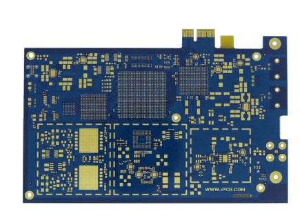
Figure2:FPGA high-speed circuit board model
High frequency PCB: Signal "vibrates frequently" - independent of switching speed
The "high frequency" in high-frequency PCB refers to the high vibration frequency of the signal itself. The industry typically considers 300 megahertz and above as "high frequency", and in some cases, even 100 megahertz and above need to be treated as high frequency PCBs. These types of signals are mostly analog signals, such as 5G signals or radar waves, with smooth sinusoidal waveforms (without sharp "switching"). For example, the millimeter wave used in 5G base stations has a frequency of 24 gigahertz or higher - a very high vibration frequency, and the PCB used is a high-frequency PCB.

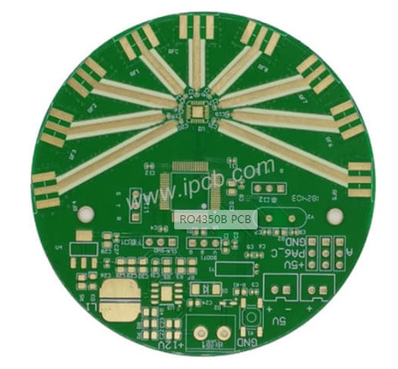
Figure1::Rogers RO4350B High Frequency Board Model
The key here is "vibration frequency": even if the signal vibration is gentle (without sharp switching), as long as the vibration is frequent enough (high frequency), it belongs to the application scenario of high-frequency PCB.
Different design goals: one to prevent "signal errors" and one to prevent "signal attenuation"
Due to the different characteristics of their signals, the design focus of high-speed PCBs and high-frequency PCBs is completely different - even completely opposite.
High speed PCB: Ensure clear and timely digital signals
Rapid switching of digital signals during transmission in PCB can cause various "confusions":
1. The steep edge of the signal may be smoothed out, causing the receiving end to be unable to distinguish between high and low levels.
2. Adjacent signals may interfere with each other (crosstalk) - when one signal switches, the other will also fluctuate accordingly.
3. The signal may reflect back from the end of the wire, forming a chaotic superimposed waveform.
4. Noise generated by power or grounding may overwhelm the signal, making it unreadable.
These issues can cause the "information" conveyed by the signal (such as 0 and 1) to become confused. If not resolved, the computer may crash and the phone may freeze.
Therefore, the design focus of high-speed PCBs is to "ensure clear signal information", and specific measures include:
1. Control the "impedance" of the wire: The "impedance" of the wire (similar to the resistance of high-speed signals) must match the impedance of the chip output and receiving ends. This is like ensuring that the thickness of the water pipe matches the faucet - avoiding water backflow and thus preventing signal reflection.
2. Carefully plan wire routing: For example, memory wires adopt a "Fly by" layout, and the length of PCIe differential pairs (paired wires) must be almost identical (with an error of within 5 mils). This ensures that the signal reaches the receiving end simultaneously, avoiding confusion at the receiving end.
3. Good grounding and shielding: Using a complete power/grounding "plane" (large metal layer) can reduce noise. Wrap sensitive wires such as clock signals with grounding wires to block interference from adjacent wires.
4. Matching wire length and signal speed: If the wire length exceeds 1/10 of the signal wavelength, a special "transmission line" design is required - otherwise the signal will be severely distorted.
High frequency PCB: Ensure that analog signals are "strong and concentrated"
High frequency analog signals (especially radio frequency or microwave signals) have another problem: * * energy loss and leakage * *. The wavelength of high-frequency signals is very short - the wavelength of a 1 GHz signal is about 30 centimeters, and the wavelength of a 10 GHz signal is only about 3 centimeters! When they are transmitted in the PCB, energy is lost through the board, copper foil, and even the gap between the copper foil and the board. At the same time, they can also leak through PCB edges or wires (causing interference) and be affected by external noise.
These issues can lead to signal attenuation or "dirtiness". If not resolved, the phone may lose signal and the radar may misjudge the distance.
Therefore, the design focus of high-frequency PCBs is on "saving energy and preventing leakage", and specific measures include:
1. Choose low loss materials: Ordinary FR-4 PCB has excessive energy loss at high frequencies. High frequency PCBs require materials such as Rogers RO4350 or Teconi TLY-5, which can reduce energy loss during signal transmission.
2. Optimize the surface of copper foil: High frequency signals mainly flow on the surface of copper foil (skin effect). If the surface of the copper foil is rough, the transmission path of the signal will become longer and energy loss will increase. Therefore, high-frequency PCBs use ultra smooth "low profile" copper foil, even silver or gold plated.
3. Design special wire structures: High frequency signals use structures such as microstrip lines, strip lines, or coplanar waveguides. The dimensions of these structures (width, plate thickness, etc.) are precisely designed to maintain impedance stability and reduce leakage - for example, the ground plane of a coplanar waveguide is close to the signal line, resulting in less signal leakage.
4. Shielding and sealing: Place a metal cover above the high-frequency circuit and drill a row of grounding holes at the edge of the PCB to prevent leakage. Some PCBs even mix materials - low loss materials are used for high-frequency parts, and cheap FR-4 is used for low-frequency parts to save costs.
3、 Different material choices: 'sufficient' and 'customized'
Materials are the key to achieving design goals, and the material choices for the two types of PCBs are also vastly different.
High speed PCB: ordinary materials (slightly upgraded)
Most high-speed PCBs, such as those found in smartphones, computers, or industrial equipment, do not require "metamaterials" - they simply need to strike a balance between cost and basic performance
1. PCB substrate: ordinary "improved FR-4" is sufficient. For example, "medium Tg FR-4" (Tg ≥ 150 ° C) has good heat resistance during welding, while "low Dk FR-4" has stable electrical properties and can avoid impedance changes. This type of material has a cost similar to regular FR-4 (80-150 yuan/square meter) and is suitable for most high-speed signals (such as PCIe 3.0/4.0, DDR4/5).
2. Copper foil: Standard electrolytic copper foil is sufficient. For ultra high speed signals (such as PCIe 5.0 and above, with a switching time of less than 0.5 nanoseconds), "low profile copper foil" (smoother) can reduce signal distortion.
3. Solder resist: Ordinary photosensitive ink is sufficient - just ensure uniform coating (uneven solder resist will change impedance).
Better materials (such as low loss FR-4 or a small amount of high-frequency materials) are only needed in ultra high speed scenarios (such as 100Gbps and above optical modules), but cost remains a key consideration.
High frequency PCB: specialized materials (higher cost)
High frequency PCBs must use materials that can minimize energy loss to the greatest extent possible - there are no shortcuts:
1. PCB substrate: It must be a material with "low Dk, low Df" (Dk is the dielectric constant, Df is the loss factor). Dk needs to be stable (2.2-3.5, with little frequency variation), and Df must be ≤ 0.005 (the higher the frequency, the lower the requirement - for example, millimeter wave requires Df ≤ 0.002). The cost of materials such as Rogers RO4350 or Teconi TLX-8 is 5-20 times that of FR-4 (500-2000 yuan/square meter).
2. Copper foil: "Extremely low profile copper foil" (super smooth) is standard. For ultra-high frequency scenarios (such as millimeter waves at 28 GHz and above), silver plated copper foil is better - silver has good conductivity and a smooth surface, which can reduce losses.
3. Other auxiliary materials: The solder resist must be of the "high-frequency low loss type" (such as solar ink SF-100) to avoid additional energy loss. Through hole electroplating requires the use of a thick gold coating - gold has stable conductivity, resulting in less energy loss at the through hole.
This is also the reason why high-frequency PCBs have higher costs - material costs alone account for 30-60% of their total cost (while the material cost of high-speed PCBs only accounts for 10-20%).
Confusing point: There is overlap, but not equivalence.
In practical applications, there may be overlap between the two - for example, a 5G baseband board contains both high-speed digital signals at the gigahertz level and high-frequency RF signals. But they are still different:
1. High speed signals may contain high-frequency components: a 100 megahertz square wave (digital signal) can be decomposed into "harmonics" such as 300 megahertz and 500 megahertz. These high-frequency components may cause losses, so it is indeed necessary to check material losses in high-speed PCB design - but the main goal is still to ensure clear signal information.
2. High frequency signals are not "high-speed signals": a 10 GHz sine wave (analog signal) vibrates gently without sharp switching. It does not have the problem of "information confusion", so high-frequency PCBs do not need to pay attention to timing or crosstalk like high-speed PCBs.
The application scenarios of the two can clearly reflect their differences:
1. High speed PCB: devices used for "fast communication" of digital signals - computer motherboards (connection between CPU and memory), server backboards (communication between modules), smartphone motherboards (connection between processors and RF modules), or industrial high-speed buses (such as EtherCAT, USB 3.0).
2. High frequency PCB: Equipment used for simulating signal "long-distance/clear transmission" -5G RF module (antenna to amplifier), radar antenna board (RF signal transmission and reception), satellite communication terminal (high-frequency carrier signal transmission), or wireless base station RF front-end (signal filtering/amplification).
The key to distinguishing between the two lies in the "characteristics" of the signal:
If it is a fast switching digital signal that requires clear transmission of "information" (without confusion), then it is a high-speed PCB - using ordinary optimized materials is sufficient. If it is an analog signal of high-frequency vibration that needs to maintain strength (no loss/leakage), then it is a high-frequency PCB - specialized low loss materials need to be used.
iPCB provides professional and diverse high-frequency PCBs and high-speed PCBs, and offers professional design and materials according to your requirements and solutions. Welcome to consult.