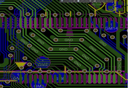
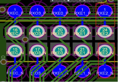
High-speed signals PCB routing, transmission line theory is essential. Some techniques differ from traditional signal routing methods. Below are some key tips for routing high-frequency signal traces.
1. Power Layout and Routing
In digital circuits, current demand is often non-continuous, leading to surge currents that can generate high-frequency noise, especially for high-speed components. If power traces are long, these surge currents can result in high-frequency noise, which may then couple into other signals.
In high-speed signal PCB routing, parasitic inductance and parasitic capacitance are inevitable. These high-frequency noises can ultimately couple into other circuits. The presence of parasitic inductance reduces the ability of the trace to handle surge currents, leading to voltage drops that may cause circuit malfunction.
Therefore, it’s crucial to add bypass capacitors near digital devices. The capacitor value should be a combination of both large and small capacitors to cover the full frequency range. Smaller capacitors should be placed as close as possible to the power supply pin of the chip. The return current path to the chip’s reference ground should be as short and wide as possible to minimize the parasitic inductance impact on high-frequency noise decoupling. Larger capacitors can be placed slightly farther from the chip, with the small capacitors positioned first.

2. Avoiding Hotspots:
Signal vias can introduce noise between power and ground layers, mainly due to parasitic inductance in the vias, which alters the return current path, potentially leading to signal return path issues and increased ground noise. Parasitic inductance in vias, in conjunction with parasitic capacitance from components (especially power devices), can cause resonance, generating high-frequency parasitic oscillations.

Improper via placement can increase current density in certain areas of the power or ground planes, resulting in hotspots. To prevent this, vias should be placed in a grid-like fashion, ensuring even current density and maintaining continuous planes, thus avoiding isolation of the ground plane and minimizing EMC (electromagnetic compatibility) issues.
3. Trace Bending Techniques
1. Bending Rules for Traces
When routing high-speed signal traces, bends are inevitable. However, it’s important to minimize the number of bends. When bending, always use rounded corners or obtuse angles, and avoid sharp or right-angle bends.

2. Serpentine Trace Design
In high-speed signal routing, serpentine traces are often used to achieve equal trace length. However, serpentine routing itself introduces bends. It is essential to properly choose trace width, spacing, and bending methods. The spacing should adhere to the 4W/1.5W rule, where "W" refers to the trace width.

4. Crosstalk Control
When high-speed signal traces are too close to each other, crosstalk can easily occur. Due to layout constraints, PCB size, etc., the minimum required spacing between traces may be exceeded. In these cases, try to increase the spacing between high-speed signal traces where possible. If space allows, it is always best to maximize the distance between traces to minimize crosstalk.
5. Stub Lines in PCB Routing
1. Stub Lines from Pull-up/Pull-down Resistors
Long stub lines act as antennas and can cause significant EMC issues. Stub lines also cause signal reflections, degrading signal integrity. Stub lines are typically generated when pull-up or pull-down resistors are added to high-speed signal traces, with the most common solution being to route the traces in a daisy-chain fashion (also known as "daisy chaining").

Experience shows that if the stub line length exceeds 1/10th of the signal wavelength, it can become problematic, effectively turning into an antenna.
2. Stub Lines at High-Speed Signal Connectors
High-speed signal connectors are common places where stub lines occur, particularly in designs with multiple connectors. The best solution is to add a series resistor near the first connector pin to mitigate stub line length. When the first connector is used, the series resistor can be switched off to reduce stub length.
Stub lines in high-speed signals not only cause reflections but also introduce impedance mismatches, as the stub line and the connecting trace act in parallel, disrupting the differential impedance.

3. Stub Lines from Automated Test Points
During automated testing, test points are often added to high-speed signal traces, creating additional stub lines. The main solutions to address this are:

Remove test points and their corresponding routing from high-speed signal traces.
Shorten the trace length between the test point and the device pin, or ideally, place the test point directly at the pin.
The iPCB has not finished sharing the high-speed signal PCB routing yet. Please check the next section.